
The Challenges to Innovate Manufacturing Industry Social demand for
Zhang, X. et al. Study of microstructural inhomogeneity and its effects on mechanical properties of multi-layer laser welded joint. Int. J. Adv. Manuf. Technol. 94, 2163–2174 (2018).
Jin, G. Q., Liang, P. & Guo, X. Y. Novel method for synthesis of silicon carbide nanowires. J. Mater. Sci. Lett. 22, 767–770 (2003).
(a) SEM image of SiC NWs; (b) TEM image of a single SiC NW with a low ODD structural occupation ratio; (c) HREM image taken from the red framed region in (b); (d) TEM image of a single SiC NW with a high ODD structural occupation ratio; (e) HREM image taken from the blue framed region in (d).
Geng, L. & Zhang, J. A study of the crystal structure of a commercial β-SiC whisker by high-resolution TEM. Mater. Chem. Phys. 84, 243–246 (2004).
Bartolo, P., Kruth, J-P., Silva, J., Levy, G., Malshe, A., Rajurkar, K., et al. (2012). Biomedical production of implants by additive electro-chemical and physical processes. CIRP Ann. Manuf. Technol. 61, 635–655. doi:10.1016/j.cirp.2012.05.005
(a)–(e) SEM images showing different single SiC NWs with different structural occupation ratio of 0%, 10.3%, 19.3%, 32.6%, 37.2%. (f) corresponding stress–strain curves of SiC NWs demonstrated in (a)–(e); (g) stress/strain-ODD occupation ratio relationship.
The authors declare that the research was conducted in the absence of any commercial or financial relationships that could be construed as a potential conflict of interest.
Wang, Fei, Shan, Chao, Yan, Jian-ping, Fu, Jiao, Garuma Abdisa, D., Zhu, T. f., et al. (2016). Application of femtosecond laser technique in single crystal diamond film separation. Diam. Relat. Mater 63, 69–74. doi:10.1016/j.diamond.2015.11.015
Materials’ mechanical properties highly depend on their internal structures. Designing novel structure is an effective route to improve materials’ performance. One-dimensional disordered (ODD) structure is a kind of particular structure in silicon carbide (SiC), which highly affects its mechanical properties. Herein, we show that SiC nanowires (NWs) containing ODD structure (with an occupation ratio of 32.6%) exhibit ultrahigh tensile strength and elastic strain, which are up to 13.7 GPa and 12% respectively, approaching the ideal theoretical limit. The ODD structural occupation ratio effect on mechanical properties of SiC NWs has been systematically studied and a saddle shaped tendency for the strength versus occupation ratio is firstly revealed. The strength increases with the increase of the ODD occupation ratio but decreases when the occupation ratio exceeds a critical value of ~ 32.6%, micro twins appear in the ODD region when the ODD segment increases and soften the ODD segment, finally results in a decrease of the strength.
Eberle, G., Dold, C., and Wegener, K. (2015). Laser fabrication of diamond micro-cutting tool-related geometries using a high-numerical aperture micro-scanning system. Int. J. Adv. Manuf. Technol. 81 (5-8), 1117–1125. doi:10.1007/s00170-015-7240-x
Geng, Z., Tong, Z., Huang, G., Zhong, W., Cui, C., Xu, X., et al. (2022). Micro-grooving of brittle materials using textured diamond grinding wheels shaped by an integrated nanosecond lasersystem. Int. J. Adv. Manuf. Technol. 1, 5389–5399. doi:10.1007/s00170-022-08695-2
Wang, C. Q. et al. Creation of controllable high-density defects in silver nanowires for enhanced catalytic property. Nano Lett. 16, 5669–5674 (2016).
Pettersson, U., and Jacobson, S. (2006). Tribological texturing of steel surfaces with a novel diamond embossing tool technique. Tribol. Int. 39 (7), 695–700. doi:10.1016/j.triboint.2005.06.004
Y.H.Y. proposed and supervised the project; X.J.Z., J.W. performed the in situ tensile tests in SEM; Z.Y.Y. performed the simulation; Y.H.Y., X.J.Z., J.W., X.K.T., analyzed data and wrote the manuscript. All authors participated in discussions of the research.
FIGURE 8. Cutting performance of SCD microscale milling tool with rake angle of −30° (ap = 0.05 mm, f = 0.143 μm/rev), (A) optical microscope image of groove, (B) SEM image of fused silica machined surface, (C) surface roughness Ra of fused silica machined surface, (D) cutting force monitor of micro-milling process.
Wang, J. F. et al. Mechanical properties and internal friction of Mg–Zn–Y alloys with a long-period stacking ordered structure at different Y/Zn atomic ratios. J. Mater. Res. 30, 3354–3362 (2015).
In order to facilitate processing, the 1 mm thick SCD sheet brazed on the front end of the carbide shank is firstly cut into a cylinder with a diameter of 1 mm as the tool blank by picosecond laser. The front end of the diamond cylinder is processed into a micro-structure with a depth of about 200 μm, forming 6 cutting-edges concentric with shank. The milling tool manufactured by this method can be regarded as composed of shank, transition section and cutting section (Figure 1), in which the latter two are processed from one diamond sheet. The welding area of the shank and transition section is far greater than the cross-sectional area of the cutting section, so such structure can bear larger cutting force and torque.
Xue, Z. G. et al. Deterministic line-shape programming of silicon nanowires for extremely stretchable springs and electronics. Nano Lett. 17, 7638–7646 (2017).
Hsu, E. M., Mailman, N. A., Botton, G. A., and Haugen, H. K. (2011). Microscopic investigation of single-crystal diamond following ultrafast laser irradiation. Appl. Phys. A 103 (1), 185–192. doi:10.1007/s00339-010-5986-4
Okamoto, Yasuhiro, Okubo, Tubasa, Kajitani, Atsuya, and Okada, Akira (2022). High-quality micro-shape fabrication of monocrystalline diamond by nanosecond pulsed laser and acid cleaning. Int. J. Extrem Manuf. 4, 025301. doi:10.1088/2631-7990/ac5a6a
Wang, J. et al. Influence of microstructures on mechanical behaviours of SiC nanowires: a molecular dynamics study. Nanotechnology 23, 025703 (2012).
Xiong, L. B. et al. Size-controlled synthesis of Cu2O nanoparticles: size effect on antibacterial activity and application as a photocatalyst for highly efficient H2O2 evolution. RSC Adv. 7, 51822–51830 (2017).
(a) TEM image of a single SiC NW with ODD structure occupation ratio of ~ 38%, Thompson tetrahedron showing the orientation relationship of the 4 {111} planes; (b) FFT image taken from the yellow dashed circle region in (a); (c) Enlarged HREM image taken from the pink framed region in (a); (d) and (e) are enlarged HREM images taken from the red and blue framed regions in (c), yellow lines in (e) display TBs.
Xu, F., Lu, W. & Zhu, Y. Controlled 3D buckling of silicon nanowires for stretchable electronics. ACS Nano 5, 672–678 (2011).
Yue, Y. H. & Zheng, K. Strong strain rate effect on the plasticity of amorphous silica nanowire. Appl. Phys. Lett. 104, 231906 (2014).
Where, i0 is the laser peak energy, ω is the laser radius when the laser energy drops to 1∕ⅇ times of the peak energy, r is the distance between a point in the beam and the laser center, and p is the laser path pitch.
Mouhamadali, F., Equis, S., Saeidi, F., Best, J. P., Cantoni, M., Hoffmann, P., et al. (2020). Nanosecond pulsed laser-processing of CVD diamond. Opt. Lasers Eng. 126, 105917. doi:10.1016/j.optlaseng.2019.105917
ODD structure is a kind of particular structure in SiC, which highly affects its mechanical properties. In this study, with in situ tensile tests of single SiC NWs with different ODD occupation ratios in a SEM, we demonstrated that SiC NW with an ODD occupation ratio of 32.6% exhibits an ultrahigh tensile strength and a super large elastic strain which are up to 13.7 GPa and 12%, respectively, near the ideal theoretical limit. A strong saddle shaped ODD occupation ratio effect on the mechanical properties was revealed for the first time. The strength increased with the increase of the ODD occupation ratio but decreased when the occupation ratio exceeded a critical value of ~ 32.6%, micro twins appeared in the ODD region when the ODD segment increased and softened the ODD segment, finally resulted in a decrease of the strength. This work may shed light on the strategy to modify materials’ mechanical properties by structure design.
FIGURE 3. Two laser machining path for cutting section, (A) the profiled helix of the cutting-edge contour, (B) optical microscope image of cutting edges using (A) as processing path, (C) laser processing path of fractional array machining, (D) optical microscope image of cutting edges using (C) as processing path.
Xue, Z. G. et al. In-plane self-turning and twin dynamics renders large stretchability to mono-like zigzag silicon nanowire springs. Adv. Funct. Mater. 26, 5352–5359 (2016).
This study was supported by the National Natural Science Foundation of China (51922017, 51972009), the Fundamental Research Funds for the Central Universities (YWF-19-BJ-J-94), Y. Y. was also supported by state key laboratory for Mechanical Behavior of Materials (20182003).
FIGURE 10. SCD milling tool after being used and a processing application, (A) SEM image of micro milling tool wear, (B) micro milling strategy for Fresnel lens, (C) microscale Fresnel lens array machined by laser-produced SCD milling tool and its profile.
In order to further verify the processing ability of laser processed SCD milling tool on the microstructure surface of fused silica, a microscale Fresnel lens array was processed on the optical fused silica surface. The optical refraction surface of the Fresnel lens was processed by the bottom edge of the microscale milling tool, and the non-working surface of the Fresnel lens was processed by the side edge. (Figure 10B). The specific milling tool orientation and tool center position were calculated by the normal direction of the Fresnel lens surface and the machining process was carried out on the CNC five-axis machining center. As shown in Figure 10 c, three Fresnel lenses with aperture of 1.6 mm and focal length of 8 mm were completed with a laser-processed diamond milling tool with negative rake angle of −30°. Figure 10C shows the optical microscope image of one Fresnel lens and its cross-section measured by surface profile instrument. The bright and clear focus spot indicate that the processed Fresnel lens has high-precision profile and good surface finish.
After continuous milling of fused silica with laser-machined SCD microscale milling tool for 22 min (ap = 0.05 mm, f = 0.143 μm/rev), the machined surface roughness Ra has increased from 44 nm to 67 nm. Tool wear was evaluated by SEM image (Figure 10A). It is found that the tool wear mainly occurred at the rake face near the bottom edge and the side edge, in terms of chipping of the tool tip and the flaky peeling of rake face. According to the diameter of tool cutting section, continuous working time and spindle speed, the maximum cutting length of the tool tip on diamond milling tool with rake angle of −30° can be estimated as 967.6 m when used for fused silica milling with cutting depth of 0.05 mm and feed per revolution of 0.143 μm. Such microscale tool life can ensure that the machining of micro-structure with small machining range can be completed without switching tools.
Wu, Mingtao, Guo, Bing, Zhao, Qingliang, He, Ping, Zeng, Z., and Zang, J. (2018). The influence of the ionization regime on femtosecond laser beam machining mono-crystalline diamond. Opt. Laser Technol. 106, 34–39. doi:10.1016/j.optlastec.2018.03.031
The profile of SCD milling tool processed by direct machining strategy and fractional array machining strategy is measured and analyzed by optical microscope. Figure 3B shows the morphology of all cutting edges processed with direct machining strategy. Due to the continuous laser ablation for a long time, a large number of thermal defects including cracks and fragmentation appear on the diamond surface, the cutting edges are not sharp, and the profile of the cutting edge is seriously poor. The centers of the two concentric circles in Figure 3B are the axis positions of the cylindrical shank, and the two circles are the maximum and minimum rotation circles of the cutting edges, respectively. The radius difference between the two circles is defined as total radial runout of the cutting edges. The eccentricity between the geometric center of cutting edges and the shank axis is measured as 8 μm. Due to the position error of the shank in the laser processing system and serious laser-induced processing defects, the total radial runout of the six cutting edges is 26 μm. Such a large runout makes the cutting edges unable to fully participate in cutting and unstable actual feed per tooth will lead to poor processing effect of brittle materials.
For these two kinds of SiC segments, comparing with triditional 3C structure, ODD segment could be consided as a kind of hard phase while 3C structure was considered as the soft phase, as revealed in nacre or manmade nacre-like materials32,33, the ratio between hard phase and soft phase is esstional to the mechanical properties of composites34,35. When the hard phase proportion increased, the strength increased but would result in a decrease of the total strain as shown in Fig. 4g. But why the strength displays a saddle like tendency with the ODD occupation ratio? After we further studied the structure of the large ODD segment, we found the reason that also originated from the interior structure of the ODD. Figure 5a shows a TEM image of single SiC NW with an ODD occupation ratio of ~ 38%. High density ODD regions were demonstrated clearly. After we enlarged the pink framed region as shown in Fig. 5b, we found that besides the high density ODD structure (Fig. 5c), there were also many micro-twins existing within the ODD structure as shown in Fig. 5d, with the highest thickness approached ~ 2 nm. As mentioned in previous study36, angstrom-scaled twins (0.7 nm in thickness) could help materials approach its theoretical strength, but, homogeneous nucleation of dislocations inside the NWs followed by shear localization and confined microplasticity at twin boundaries (TBs) would occurred when the twin thickness increased, leading to an increase of strain but a decrease of the strength. Herein, the appearance of micro-twins in ODD structure finally decreased the strength of the ODD structure, the total strain of SiC NWs with a higher ODD occupation ratio had hit bottom and begun climbing again as shown in Fig. 4g, displaying a contrary tendency to the tendency of strength.
Due to the inertia of the optical element that controls laser spot position, the scanning speed of laser at the abrupt change-point of the processing path will be reduced, and the long-time stay of laser makes excessive material removal, as a result, it is not easy for laser beam machining to process sharp features. Considering that the cutting-edges need to be sharp enough to ensure good processing performance, the rake and flank face of the milling tool are processed separately and form the cutting edges to avoid the long-time stay of laser and obtain a fine cutting-edge profile. As shown in Figure 3C, the chip removal groove and the flank face are processed by the laser with the red processing path, and then the rake face is finished by the laser according to the blue processing path, and the cutting edge is formed.

Luo, W. & Bazant, Z. P. Fishnet model for failure probability tail of nacre-like imbricated lamellar materials. Proc. Natl. Acad. Sci. U. S. A. 114, 12900–12905 (2017).
Springer Nature remains neutral with regard to jurisdictional claims in published maps and institutional affiliations.
Zhang, H. T. et al. Approaching the ideal elastic strain limit in silicon nanowires. Sci. Adv. 2, e1501382 (2016).
Wegst, U. G. K., Bai, H., Saiz, E., Tomsia, A. P. & Ritchie, R. O. Bioinspired structural materials. Nat. Mater. 14, 23–26 (2015).
For the hard and brittle material such as fused silica, in addition to the correct cutting parameters, the tool needs to have a negative rake angle to suppress the generation of cracks, and needs a high stiffness design to resist cutting vibration and tool deformation. Allowing for working depth and stiffness of the milling tool, the diameter and length of cutting section on the proposed microscale diamond milling tool are designed as approximately 400 μm and 200 μm respectively. And due to the low feed per tooth in the machining process of hard and brittle materials, the milling tool with high concentric multiple cutting edge is attractive because of high material removal rate.
Zheng, K. et al. Electron-beam-assisted superplastic shaping of nanoscale amorphous silica. Nat. Commun. 1, 24 (2010).

Kumar, Sumit, Tong, Zhen, and Jiang, Xiangqian (2022). Advances in the design and manufacturing of novel freeform optics. Int. J. Extrem Manuf. 4, 032004. doi:10.1088/2631-7990/ac7617
Konov, Vitaly I. (2012). Laser in micro and nanoprocessing of diamond materials. Laser Photonics Rev. 6 (6), 739–766. doi:10.1002/lpor.201100030
Zhang, X., Wang, J., Yang, Z. et al. Strong structural occupation ratio effect on mechanical properties of silicon carbide nanowires. Sci Rep 10, 11386 (2020). https://doi.org/10.1038/s41598-020-67652-9
The optimal pitch of laser processing paths po should meet the minimum error of laser energy fluctuation. Figure 2B shows the impact of overlap of laser processing paths on energy fluctuation. When the pitch of laser processing path is 1.56ω, the fluctuation error of accumulated absorbed laser energy on the ablated surface is the lowest, and the theoretical value is 1.48%.
Figure 9 shows the test result of roughness Ra obtained with surface profile instrument. The experimental results show that the fused silica processed with the negative rake angle tool has lower surface roughness, and the negative rake angle tool is suitable for milling process of fused silica. Moreover, a more obvious negative rake angle can produce a surface with lower roughness, under the conditions of all feed rates in the cutting experiment. When the feed rates are 5 mm/min and 10 mm/min, the milling tool with rake angle of 5° has better cutting performance than the tool with 0° rake angle at the beginning of milling, but the sharp wear of the positive rake angle tool when machining hard and brittle materials causes the rapid deterioration of the cutting-edge state, making its service life very short.
Shi, Y., Yang, S. H. & Xing, D. Quantifying the plasmonic nanoparticle size effect on photoacoustic conversion efficiency. J. Phys. Chem. C 121, 5805–5811 (2017).
Ryu, S. Y. et al. Lateral buckling mechanics in silicon nanowires on elastomeric substrates. Nano Lett. 9, 3214–3219 (2009).
FIGURE 5. Experimental apparatus for cutting performance verification of SCD microscale milling tool.
In our tesile tests, all tested SiC NWs demonstrated a brittle-like fracture feature. Take Fig. 5a as an example, the force loading direction is along [11−1]. Stacking sequence in 3C-SiC segments was ABCABC…(A, B, C represents the three basic structure modules of tetrahedral bonding in SiC37), creating a straight atomic plane along all of the 4 {111} planes ((1−11), (11−1), (111) and (−111) plane (as demonstrated in Fig. 5b) which were translational symmetry and periodicity in these four {111} planes, and the green tetrahedron in Fig. 5a demonstrated the Thompson tetrahedron, showing the orientation relationship of these four {111} planes. However, stacking sequence in the ODD structure was in a random order, such as ACABABCB…, the translational symmetry and periodicity were broken in the three sets of (1−11), (111), and (−111) planes except for the (11−1) plane. When yielding happened, free surface in ODD structure possessed high energy and would act as dislocation source to emit dislocations, but all the three sets of (1−11), (111), and (−111) sliding planes were broken due to the discontinuous slipping plane, dislocation emission along these three planes was almost impossible. Furthermore, the force loading direction was vertical to (11−1) plane, and all types of dislocations on (11−1) plane including full dislocations along 〈110〉 and partial dislocations along 〈112〉 had a Schmid factor of zero which was impossible for dislocation movement in (11−1) plane, so dislocation behavior could be found only in 3C segments under a low strain rate as report before9. If the tensile test was conducted at a high strain rate, stress concentration was fast enough to form a crack on the ODD segment surface and brittle fracture would happen28 under such a high strain rate of 10−3 s−1. Such brittle fracture phenomenon shown in Fig. 2 and Supplementary Fig. S3 (See more details in Movie S3) were further confirmed by the MD simulation result as demonstrated in Fig. 6, a constant tensile force was loaded to the SiC NW with a strain rate of ~ 108 s−1. The nanowire was constructed according to the experimental result with an ODD occupationa ratio of 33.3% to study the fracture mode. Figure 6a–d demonstrate a cleavage fracture model which was in accordance with our experimental results, small crack appeared near the ODD/3C interface region as shown in Fig. 6b, where no obvious dislocation behavior were found during the fracture process and the crack propagated rapidly to another side of the nanowire, resulting in a brittle failure as shown in Fig. 6d. In order to prove our speculation mentioned above, twin lamella were inserted into the ODD region and similar tensile test was conducted as shown in Supplementary Fig. S4. As predicted, fracture happened in the twin lamellae with the same fracture model as shown in Fig. 6 but with a slight decrease in strength (see Supplementary Fig. S4 online), in accord with our experimental result, further proved our interpretation of the strong ODD occupation effect on the strength of SiC NWs.
Zhou, Tianfeng, He, Yupeng, Wang, Tianxing, Zhu, Zhanchen, Xu, R., Yu, Q., et al. (2021). A review of the techniques for the mold manufacturing of micro/nanostructures for precision glass molding. Int. J. Extrem Manuf. 3, 042002. doi:10.1088/2631-7990/ac1159
Li, J. H. et al. Synthesis, characterization and field emission properties of SiC nanowires prepared by chemical vapor reaction. Vacuum 146, 87–92 (2017).
Han, X. D. et al. Polarization driven covalently-bonded octahedral-twinning and backbone-peripheral-helical nanoarchitectures. Nano Lett. 8, 2258–2264 (2008).
During the tensile tests of SiC NWs, we found that the strength varies greatly with the change of the ODD occupation ratio. In order to map out the relationship between the ODD occupation ratio and the mechanical properties, SiC NWs with different ODD occupation ratios but with similar diameter have been picked up to conduct the tensile tests. Selecting nanowires with similar diameter aims to rule out the size effect on the mechanical properties31, then, the difference in mechanical properties is mainly due to structural changes. Figure 4a–e demonstrates 5 single SiC NWs with different ODD occupation ratios which are ranging from 0 to 37.2%. The occupation ratio was calculated according to the volume fraction of the ODD segments. All corresponding stress–strain curves of these SiC NWs are presented in Fig. 4f. Most of these stress–strain curves demonstrate good linearity. The strength increased with increasing of the ODD occupation ratio at the beginning but decreased when the occupation ratio was higher than 32.6%, and the highest strength was approaching ~ 13.7 GPa, near the therotical strength limit27. Curiously, the strength didn’t increase with further increase of the ODD structural occupation ratio after the critical value of 32.6%, it decreased when the ODD occupation ratio was higher than this value and a saddle like ODD occupation ratio effect on the strength was first demonstrated as shown in Fig. 4g. Different with the tendency strength, the strain demonstrated a antipodal tendency comparing with the strength, it decreased with increasing of the ODD structural occupation ratio and increased when the occupation ratio reached higher than 32.6% as shown by the red line in Fig. 4g.
SCD is prone to graphitization at high temperature, and this change in atomic distribution will greatly damage the performance of diamond tools. In addition to the geometric characteristics of the tool, the graphitization of the tool surface needs to be monitored for the diamond tool made by laser. Considering that diamond and graphite have different characteristic peaks, Raman spectroscopy can analyze the graphitization degree of the SCD surface. Laser with wavelength of 633 nm and power of 17 mW was used as light source for Raman spectroscopic investigation. And the measuring position was the side edge of the milling tool, which has the longest laser ablation time and has an important impact on the cutting performance.
The profile accuracy and concentricity of the cutting-edges are important indicators to determine the cutting performance. Considering that the eccentricity between the laser processing path and the shank caused by its position error in the laser processing system is difficult to avoid, the processing path needs to be optimized so that the cutting-edge runout is not affected by the shank position. The fractional array machining will help to suppress the cutting-edge runout caused by the position error of the shank. In one process of laser ablation, only one cutting edge is processed, and then the same processing path is used to process another after the shank is rotated until all cutting edges are processed (Figure 3C). Using this processing strategy, the center of the circular array of the processing path is the axis of the shank. Therefore, the position error of the shank in the laser processing system only slightly affects the diameter of cutting section on milling tool, and does not affect the radial runout of the cutting-edges.
We conducted the in situ tensile tests of single SiC NW by a Pico Indenter (Pi-85 from Bruker) in a SEM at an accelerate voltage of 10 kV. FIB was employed to transfer and fix the single SiC NW onto the PTP device. We use the displacement control mode to pull the single SiC NW until its fracture at a displacement rate of 2 nm s−1. The force VS displacement curve accompanied by the real-time video were recorded dynamically.
The original contributions presented in the study are included in the article/supplementary material, further inquiries can be directed to the corresponding author.
Tong, Zhen, Luo, Xichun, Sun, Jining, Liang, Yingchun, and Jiang, Xiangqian (2015). Investigation of a scale-up manufacturing approach for nanostructures by using a nanoscale multi-tip diamond tool. Int. J. Adv. Manuf. Technol. 80, 699–710. doi:10.1007/s00170-015-7051-0
Shinoda, M., Gattass, R. R., and Mazur, E. (2009). Femtosecond laser-induced formation of nanometer-width grooves on synthetic single-crystal diamond surfaces. J. Appl. Phys. 105 (5), 053102. doi:10.1063/1.3079512
Cao, A., Wei, Y. G. & Ma, E. Grain boundary effects on plastic deformation and fracture mechanisms in Cu nanowires: molecular dynamics simulations. Phys. Rev. B 77, 195429 (2008).
Yang, T., Chang, X. W., Chen, J. H., Chou, K. C. & Hou, X. M. B-doped 3C-SiC nanowires with a finned microstructure for efficient visible light-driven photocatalytic hydrogen production. Nanoscale 7, 8955–8961 (2015).
Nan Lia, Hao, Xie, Ke Ge, Wu, Bo, and Zhu, Wei Qiang (2020). Generation of textured diamond abrasive tools by continuous-wave CO2 laser: Laser parameter effects and optimisation. J. Mater Process Technol. 275, 116279. doi:10.1016/j.jmatprotec.2019.116279
Oliveira, J. B., Morbec, J. M. & Miwa, R. H. Mechanical and electronic properties of SiC nanowires: an ab initio study. J. Appl. Phys. 121, 104302 (2017).
FIGURE 7. Raman spectrum of diamond milling tools machined with two laser processing paths, (A) the profiled helix of the cutting-edge contour, (B) fractional array machining.
High quality SiC NWs were prepared by the carbothermal reduction of the carbonaceous silicon xerogels containing lanthanum additive25,26. Figure 1a demonstrates the general morphology of the SiC NWs under scanning electron microscopy (SEM) observation. The average SiC NWs have a length of dozens of microns and with diameters ranging from several tens of nanometers to ~ 200 nm. Figure 1b shows a transmission electron microscopy (TEM) image of a single SiC NW consists of two type intergrowth segments as indicated by “A” and “B”, where segment “A” has smooth surface but segment “B” looks like a bamboo joint with rough surfaces8. With high resolution electron microscopy (HREM) image (Fig. 1c) taken from the red framed region in Fig. 1b, we find that segment “A” is the FCC structure, but segment “B” possesses ODD structure along 〈111〉 direction with stacking-faulted sequence of {111} plane which is along the longitude growth axis of the NW, insert in Fig. 1c shows the fast Fourier transform (FFT) image taken from the yellow framed region in Fig. 1c. Elongated spots in the insert image indicates the existence of the stacking-faults as demonstrated in Fig. 1c. Similar as Fig. 1b, d shows another single SiC NW but with a high ODD occupation ratio comparing with Fig. 1b. Figure 1e shows the HREM image taken from the blue framed region in Fig. 1d, and higher density ODD structure is further confirmed by the elongated spots which is nearly a line as shown in the FFT image (insert in Fig. 1e). In order to quantify the effect induced by the ODD segments, in situ tensile tests of single SiC NWs with different ODD structural occupation ratios have been conducted in SEM.
Malayath, Ganesh, Sidpara, Ajay M., and Deb, Sankha (2020). Fabrication of micro-end mill tool by EDM and its performance evaluation. Mach. Sci. Technol. 24 (2), 169–194. doi:10.1080/10910344.2019.1636269
Han, X. D. et al. Low-temperature in situ large strain plasticity of ceramic SiC nanowires and its atomic-scale mechanism. Nano Lett. 7, 452–457 (2007).
FIGURE 2. Effect of laser path overlap on the flatness of machined surface, (A) ablated surface formation process using laser layered cutting, (B) the influence of Gaussian laser beam overlaps on the fluctuation of accumulated energy.
Open Access This article is licensed under a Creative Commons Attribution 4.0 International License, which permits use, sharing, adaptation, distribution and reproduction in any medium or format, as long as you give appropriate credit to the original author(s) and the source, provide a link to the Creative Commons license, and indicate if changes were made. The images or other third party material in this article are included in the article's Creative Commons license, unless indicated otherwise in a credit line to the material. If material is not included in the article's Creative Commons license and your intended use is not permitted by statutory regulation or exceeds the permitted use, you will need to obtain permission directly from the copyright holder. To view a copy of this license, visit http://creativecommons.org/licenses/by/4.0/.
The authors acknowledge for the support from the National Natural Science Foundation of China under the Grant Nos. U20A20284 and 52075323.
To demonstrate the cutting performance of laser shaped tools, micro-milling tests on fused silica were conducted under different cutting conditions. The effects of rake angle on cutting force and the degree of brittle damage on the subsurface of fused silica are studied. After machining, the machined fused silica surfaces are observed by optical microscope and scanning electron microscope (SEM, Tescan). The SEM image of Figure 8B indicate that the machined surface of fused silica is not smooth, but has sub-micron to micron size crushing without obvious cracks. The cutting force of micro-milling was also monitored and recorded in real time. The result shows that the amplitude of cutting force is stable and no tool fracture occurs. The cutting force increases slightly when the cutting tool with negative rake angle is used. Table1 shows the amplitude of cutting force using different rake angles and feed rates. Cutting force is mainly affected by the feed rate. In the cutting performance experiment, the cutting force is basically proportional to the feed rate.
Fused silica is widely used as a material for optical lenses owing to its excellent optical properties and low thermal expansion coefficient. However, as a hard and brittle material, there is very limited option of processing technologies to machining fused silica with surface structures. In this paper, a picosecond laser based single crystal diamond tool fabrication technology is proposed to generate micro milling tools with different geometrical designs, and the tool cutting performance is experimentally tested through micro-milling of fused silica under different cutting conditions. An optimal picosecond laser processing path is proposed to inhibit the graphitization of diamond tool and improve the concentricity of tool blades, and a multi-edge milling tool with a minimum rotary diameter of 0.4 mm can be obtained. The effects of rake angle on cutting force and the degree of brittle damage on the subsurface of fused silica are studied by micro milling tests of fused silica using the laser-shaped tools. The results show that the fused silica machined by diamond milling tool with a rake angle of −30° has the best surface finish (Ra = 41.2 nm). Using this laser-machined milling tool, a plurality of micro Fresnel lenses with aperture of 1.6 mm were successfully machined on a fused silica sheet.
The cutting test of the microscale milling tool is carried out on the precision 5-axis machining center Kern Micro. The milling tool produced by picosecond laser is installed on the milling spindle with the maximum rotational speed of 50000 rpm and radial runout of less than 0.8 μm by HSK tool holder. The linear feed axis of the machine tool is driven by a linear motor, which can realize the stable movement of low feed speed with positioning accuracy of 1 μm and repetitive positioning accuracy of 0.5 μm. The two rotation axes of the machine tool are B and C axes, with positioning accuracy of 0.002° and their axes are parallel to Y and Z-axes respectively (Figure 5). The workpiece used for milling tool cutting performance test is a 1 mm thick fused silica sheet with Mohs hardness of 7. The fused silica sheet is fixed on the force-measuring device installed in the machine tool through the clamp, which can detect and store the cutting force data of fused silica specimen in real time. In the milling experiment, each milling tool was used with spindle speed of 35000 rpm, cutting depth of 0.05 mm and three different feed rates of 5, 10 and 15 mm/min.
Meng, F., Zhou, R., Davis, T., Cao, J., Wang, Q. J., Hua, D., et al. (2010). Study on effect of dimples on friction of parallel surfaces under different sliding conditions. Appl. Surf. Sci. 256 (9), 2863–2875. doi:10.1016/j.apsusc.2009.11.041
Richter, G. et al. Ultrahigh strength single crystalline nanowhiskers grown by physical vapor deposition. Nano Lett. 9, 3048–3052 (2009).
Chen, Li, Piao, Yinchuan, Zhang, Feihu, Zhang, Yong, Hu, Y., and Wang, Y. (2022). Understand anisotropy dependence of damage evolution and material removal during nanoscratch of MgF2 single crystals. Int. J. Extrem Manuf. 5, 015101. doi:10.1088/2631-7990/ac9eed
The laser processing depth of cutting-edges and transition section is beyond the working range of picosecond laser (depth of field), so layered cutting is applied to laser machining process, which means that laser continuously focuses and ablates the surface formed by previous processing. The Gaussian distribution of laser energy makes the laser ablation remove the material unevenly. And when laser is irradiated on an uneven surface, the projection of circular laser spot on the ablated surface is irregular, which results in a great difference in the energy density of picosecond laser ablation in different regions. Using a laser processing path with a specific overlap ratio can obtain a relatively flat laser processed surface for subsequent laser ablation (Figure 2A).
By submitting a comment you agree to abide by our Terms and Community Guidelines. If you find something abusive or that does not comply with our terms or guidelines please flag it as inappropriate.
In this work, a picosecond laser based single crystal diamond tool fabrication technology is proposed to generate micro milling tools. A series of experimental tests have been carried out to investigate the feasibility of using picosecond laser in shaping SCD multi-edge microscale milling tool, optimal laser processing parameters, and the tool cutting performance under various cutting conditions. The conclusions are summarized as follows.
Aurich, J. C., Reichenbach, I., and Schuler, G. M. (2012). Manufacture and application of ultra-small micro end mills. CIRP Ann. Manuf. Technol. 61, 83–86. doi:10.1016/j.cirp.2012.03.012
The Raman shift peaks at 1,333 cm-1 (ID) and 1,580 cm-1 (IG) correspond to the sp3 and sp2 hybridization of carbon atoms, respectively, and the intensity of peaks represents the content of SCD and graphite. The intensity ratio ID/IG of characteristic signals of diamond and graphite can be used to analyze the degree of graphitization (Wu et al., 2018). The intensity ratio of the diamond tool machined with the direct processing strategy is 1.32, while the intensity ratio of the diamond tool processed according to the fractional array strategy is 1.76 (Figure 7). The optimized processing strategy and laser processing path can reduce the graphitization of SCD in laser processing, and the SCD microscale milling tool with fine profile accuracy can be manufactured by picosecond laser.
Bouville, F. et al. Strong, tough and stiff bioinspired ceramics from brittle constituents. Nat Mater. 13, 508–514 (2014).
MD simulation result of the SiC nanowire with periodical ODD structure, the ODD occupation ratio is 33.3%. (a)–(d) show the extracted snapshots taken from the tensile process, the two orange shadow areas indicate the ODD regions.
Copyright © 2023 Song, Tong, Yao and Jiang. This is an open-access article distributed under the terms of the Creative Commons Attribution License (CC BY). The use, distribution or reproduction in other forums is permitted, provided the original author(s) and the copyright owner(s) are credited and that the original publication in this journal is cited, in accordance with accepted academic practice. No use, distribution or reproduction is permitted which does not comply with these terms.
Furthermore, the accumulated absorbed laser energy IS on the ablated surface between adjacent machining paths can be approximately expressed as the following expression.
Improving materials’ properties by designing novel structure is the most common method, therefore, it is vital to study the relationship between the structure and materials’ mechanical properties. Over the past two decades, SiC material has raised widespread concern due to its advantages such as large band gap, high thermal conductivity, high thermal stability, oxidation resistance, corrosion resistance and so on1,2,3,4. However, due to the lack of ductility at room temperature, its application has been dramatically limited. Recently, size effect is proved to be an effective strategy to improve materials’ properties5,6,7. For example, super-plasticity with local strain up to 200% in SiC nanowires (NWs) was observed8,9, similar phenomenon was revealed in other covalent system10. Besides the size effect, it is generally believed that materials’ mechanical properties critically depend on their internal structures at different length scales11,12,13. Both experimental and simulation results show that introduction of twin boundaries, grain boundaries and other internal structures can dramatically affect the mechanical properties of one-dimensional (1-D) materials14,15,16. For SiC NWs, they usually contain well-developed cubic (3C) structured segments, stacking faults, and also H-type structured segments and even helical structure17, dramatically affecting their mechanical properties, that may be the reason why the Young’s modulus of SiC NWs vary widely18. Recently, reserachers demonstrated that the stretchability of traditional brittle materials can be enhanced by buckling and channel guiding strategy19,20,21,22. Besides the structure mentioned above, one-dimentional disordered (ODD) structure with high density defects is another ubiquitous structure not only in SiC but also in other materials8,23,24, the symmetry and periodicity of the original face-centered cubic structure of SiC in the ODD structure change thoroughly8, which is considered to have not only great effect on mechanical properties but also on catalytic performance24. However, the mechanism how this structure affect the mechanical properties is still obscure. Herein, in situ tensile tests of single SiC NWs with different ODD occupation ratios (which are defined by the ODD structure volume ratios) have been conducted and a strong structure occupation ratio effect on mechanical properties is revealed for the first time. The strength increases with increase of ODD structural occupation ratio and then decreases when the occupation ratio approaches 36.2% with a maximum strength of 13.7 GPa, a saddle-shaped relationship strength versus ODD structural occupation ratio curve is demonstrated. Loading–unloading tensile tests show that the maximum elastic tensile strain of SiC NWs is ~ 12%, approaching its theoretical strain limit. Micro twins appear in the ODD region when the ODD segment increases and soften the ODD segment, finally results in a decrease of the strength. This work provides new insights into the structure effect on the mechanical properties of nanomaterials, and will be helpful for improving mechanical properties of new materials via structural design.
Thank you for visiting nature.com. You are using a browser version with limited support for CSS. To obtain the best experience, we recommend you use a more up to date browser (or turn off compatibility mode in Internet Explorer). In the meantime, to ensure continued support, we are displaying the site without styles and JavaScript.
Wang, L. H. et al. In situ atomic-scale observation of continuous and reversible lattice deformation beyond the elastic limit. Nat. Commun. 4, 2413 (2013).
Chae, J., Park, S. S., and Freiheit, T. (2006). Investigation of micro cutting operations. Int. J. Mach. Tools Manuf. 46, 313–332. doi:10.1016/j.ijmachtools.2005.05.015
Loading–unloading experiments were performed under SEM to confirm that the SiC nanowire strain could be fully recovered after very large strains were experienced upon unloading. Four loading–unloading cycles were performed on a single SiC NW with an ODD structural occupation ratio of 20.1%, as shown in Fig. 3a, the loaded maximum strain increased gradually during these four cycles. The SiC NW finally fractured at a strain of ~ 12.2% with a fracture strength of ~ 8 GPa. As shown in Fig. 3b, all the stress–strain curves showed linear and hysteresis free shape during the loading–unloading cycles. More details could be found in Movie S2 in supporting materials. Unixal tensile tests of several SiC NWs were performed to verify the repeatability of the super large elastic strain and the measured maximum elastic strain of SiC NWs is ~ 15.5%, approaching the theoretical strain limit of semiconductor materials27. As reported in previous result28, all tested SiC NWs demonstrated a brittle-like fracture character which may mainly due to the relative high strain rate that is about 1.2 × 10⁻³ s−1, it is fast and there would be no enough time for phase transformation from crystal to amorphous which would result in a super plasticity9. Such high strain rate was too fast for the nanowire to experience a plastic process induced by bond switching and rebonding29,30.
(3) A Fresnel lens array on the surface of fused silica was successfully generated by laser-machined SCD microscale milling tool, which verified that the tool prepared by laser can manufacture optical microstructures.
Daulton, T. L. et al. Polytype distribution of circumstellar silicon carbide: microstructural characterization by transmission electron microscopy. Geochim. Cosmochim. Acta. 67, 4743–4767 (2003).
All data generated or analyzed during this study are included in this published article (and its Supplementary Information files).
In situ tensile test. (a)–(d) A sequence of snapshots taken from Movie S1 showing the tensile process of a single SiC NW; (e) Stress–strain curve of the single SiC NW.
After the cylindrical transition section is obtained, the lower surface is precisely removed by laser ablation, and the remaining material forms the cutting-edges. Based on such a processing strategy, the intuitive method is to process all cutting edges at one time with the profiled helix of the cutting section contour as the processing path (Figure 3A). In theory, the edge profile error of the processed milling tool only includes the positioning error of laser spot and the laser-induced defects, and the included angle between cutting-edges and tool profile can be guaranteed. However, the eccentricity between the laser processing path and the shank will destroy the radial runout of the cutting-edges in actual processing. In addition, the continuous laser processing causes the diamond to be heated continuously due to laser thermal effect, resulting in graphitization which seriously affects the cutting performance of the tools (Figure 3B).
In contrast, the microscale milling tool machined with fractional array processing strategy has significantly improved in terms of tool profile, cutting-edge sharpness and radial runout (Figure 6). The cutting edges with fine profile are evenly distributed, and the thermal crack is suppressed. The part of the diamond removed to get each cutting edge is marked in Figure 3C, including 6 chip removal grooves and 6 areas removed for rake face finishing. Since the fractional array machining effectively suppresses the cutting-edge runout caused by the position error of shank in laser processing, the total radial runout of cutting edges with different rake angles are 9.4 μm, 5.3 μm, 7.6 μm and 8.6 μm respectively. And the deviation of cutting section diameter is about 10 μm. The intersection of the rake faces and the flank faces form sharp cutting edges, and the radius of the edge is about 3.2 ± 2.1 μm. After laser processing of tools with theoretical rake angle of 5°, 0°, - 15° and - 30°, the actual rake angle is 6°, 0°, −16° and −29°, and the maximum error is approximately 1°. All cutting edges have a clearance angle of about 10°, which can effectively reduce the friction between the flank faces and the machined surface.
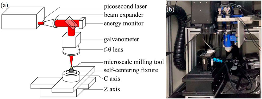
The laser processing system is composed of picosecond laser, beam expander, galvanometer, f-θ lens, energy monitor and mechanical motion axis (Figure 4). The picosecond laser (Trumpf) can produce a laser with pulse width of 8 ps, maximum average power of 40 W, base frequency of 400 kHz and beam quality M2 of up to 1.1. The beam expander increases the aperture of the parallel light generated from the laser to facilitate the generation of higher quality laser spot. The mirror in the galvanometer controlled by computer can change the direction of laser propagation, and the high-speed moving mirror in the galvanometer can provide a maximum scanning speed of 3 m/s for the laser spot movement. The laser is focused on the plane about 100 mm below the f-θ lens, which has the maximum laser energy density and is used as the working plane of picosecond laser. The energy monitor in the optical path monitors the output power of the picosecond laser in real time and feeds it back to picosecond laser to provide the correct and stable energy of the laser output. The vertical straight axis (Z-axis) can change the position of the laser working plane, and ensure that the processed area is in the focal plane of the laser during the whole laser processing. There are also two linear axes in the plane to adjust the position of the workpiece in the laser processing system. The rotation axis (C-axis) under the f-θ lens is used as the indexing head to rotate the shank which was clamped on it with a self-centering fixture.
Chen, K., Shi, B., Yue, Y. H., Qi, J. J. & Guo, L. Binary synergy strengthening and toughening of bio-inspired nacre-like graphene oxide/sodium alginate composite paper. ACS Nano 9, 8165–8175 (2015).
Citation: Song J, Tong Z, Yao Z and Jiang X (2023) Micro milling of fused silica using picosecond laser shaped single crystal diamond tools. Front. Mater. 10:1176545. doi: 10.3389/fmats.2023.1176545
Micro-structured surfaces have received increasing interests in recent years due to their wide applications in optics and electronics (Holmberg et al., 2014), bioengineering (Bartolo et al., 2012) and tribology (Meng et al., 2010). For example, Fresnel lenses or lenses with diffraction structures have irreplaceable functions of lenses with smooth surface. Micro and nanomanufacturing technologies such as laser machining, electron beam lithography, ion beam etching, nanoimprinting, etc. can fabricate those micro-lenses to some extent. Nano scratching test (Chen et al., 2022) has been reported to understanding the material deformation behavior in nanoscale. However, the large-scale production of functional microstructure surfaces is very limited due to their high production cost and low production efficiency. With the advance of tooling technology, micro milling using special designed cutting tool is recognized as a potential method to produce micro-structure with high material removal rate and good surface integrity (Chae et al., 2006; Aurich et al., 2012). Diamond is an ideal material for micro-tools because of its outstanding properties in terms of hardness, rigidity and thermal conductivity (Kumar et al., 2022).
SEM was employed to characterize the initial length and the diameter of the tested SiC NW. The stress and the strain were calculated based on the diameter and the elongation. Both the sample and the PTP device contributed to the force. Thus, we subtracted the force contributed by the PTP device to calculate the stress.
Mao, S. S., Quéré, F., Guizard, S., Mao, X., Russo, R., Petite, G., et al. (2004). Dynamics of femtosecond laser interactions with dielectrics. Appl. Phys. A 79 (9), 1695–1709. doi:10.1007/s00339-004-2684-0
(a) Loading–unloading tensile test of a single SiC NW with increasing tensile strain amplitude and full unloading in each cycle. The nanowire recovered its original length after strain values of ~ 2.1, ~ 8.0, and ~ 10.1% were experienced in each cycle and eventually fractured at the fourth cycle with a final strain of ~ 12.2%, the broken nanowire flew away as shown in the last snapshot in (a). (b) Corresponding stress-versus-strain curves of the multicycle loading–fully unloading test, different colors were used to better illustrate the data for each cycle.
JS—study, experiment, article writing ZT—participate in the study, article writing ZY—support and funding XJ—support and funding.
Uniaxial tensile tests of single SiC NWs were performed using an in situ quantitative nanoindenter (Hysitron Pi-85) inside a FEI Quanta 250 FEG SEM. A dual beam (focus ion beam, FIB-SEM) system was used to transfer and fix SiC NWs. A tungsten probe was used to pick up the target SiC nanowire and put it to the gap of the push-to-pull (PTP) device, then Pt patterns were deposited to the two ends of the SiC NW to fix it as shown in Figure S1a. The basic configuration of the tensile tests was also shown in Figure S1, after the 20 μm flat probe was positioned to touch the semi-circular end of the PTP device, the indentation force converted to tensile force and loaded to the yellow dashed line framed region as shown in Supplementary Fig. S1a. Uniaxial tensile force loaded (along the direction marked by the two yellow arrows) to the tested SiC NW that was fixed on the device by FIB. Meanwhile, the force and displacement curve and a real-time movie were recorded dynamically. The true force-versus-displacement curve of a tested sample could be accurately extracted and transferred to stress–strain curve by removing the contribution from the free PTP device (See Supplementary Fig. S2 online). Supplementary Fig. S1b displayed a single SiC NWs with lots of bamboo joints as denoted by the yellow arrow, which was fixed on a PTP device by FIB. Figure 2a–c demonstrated a sequence snapshots extracted from the Movie S1, which was captured during the tensile test of a SiC NW with an ODD structural occupation ratio of 32.6%, the maximum strain approached ~ 12%, while the calculated stress reached about 13.7 GPa as shown in the stress–strain curve in Fig. 2e, then, the SiC NW fractured and ejected without obvious plastic deformation as shown in Fig. 2d, e.
FIGURE 6. Optical microscope image of cutting edge profile for microscale milling tools with rake angle of (A) 5°, (B) 0°, (C) −15° and (D) −30°.
All claims expressed in this article are solely those of the authors and do not necessarily represent those of their affiliated organizations, or those of the publisher, the editors and the reviewers. Any product that may be evaluated in this article, or claim that may be made by its manufacturer, is not guaranteed or endorsed by the publisher.
In this paper, a picosecond laser based single crystal diamond tool fabrication technology is proposed to produce SCD microscale milling tool. The focus is on how to effectively control the laser beam for improved tool profile accuracy and its cutting performance. The effects of tool rake angle on cutting force and machined surface roughness were studied, from which optimal cutting parameters were identified. The feasibility of using the laser-shaped SCD milling tool on surface micro-structuring was demonstrated by generating a micro Fresnel lens array on fused silica surface.
Ritter, Y., Şopu, D., Gleiter, H. & Albe, K. Structure, stability and mechanical properties of internal interfaces in CuZr nanoglasses studied by MD simulations. Acta. Mater. 59, 6588–6593 (2011).
Murata, K. et al. The metal-support interaction concerning the particle size effect of Pd/Al2O3 on methane combustion. Angew. Chem. 56, 15993–15997 (2017).
Wang, J. W. et al. Near-ideal theoretical strength in gold nanowires containing angstrom scale twins. Nat. Commun. 4, 1742 (2013).
SCD transition section is machined from 1 mm thick SCD sheet by layered cutting using a group of concentric circular picosecond laser processing paths. The minimum radius rmin of this group of concentric circles is the design radius of SCD transition section, the step increment is the optimal pitch po, and the maximum radius is rmin+bmin, which meets the minimum groove width for efficient laser ablation.
We used a Quanta 250 FEG SEM to characterize the morphology of the SiC NWs. A JEOL 2100F TEM at an accelerate voltage of 200 kV was employed to study the structure of the SiC NWs.
The diamond to be laser processed is a diamond sheet synthesized by means of high temperature and high pressure (HPHT), with thickness of 1.0 mm. The microscale milling tools with rake angle of 5°, 0°, −15°, −30° and clearance angle of 10° are processed by picosecond laser with average laser power of 4 W, scanning speed of 0.5 m/s and the predetermined processing path, and prepared for cutting performance testing.
Holmberg, S., Perebikovsky, A., Kulinsky, L., and Madou, M. (2014). 3-D micro and nano technologies for improvements in electrochemical power devices. Micromachines. 5, 171–203. doi:10.3390/mi5020171
The preparation of high-quality single crystal diamond (SCD) microscale milling tool is the key of micro milling using micro-tool. As the hardest material, micro diamond tool is difficult to fabricate in conventional grinding process (Mouhamadali et al., 2020). Several new processing methods have been applied to produce microscale diamond tools, such as electric discharge machining (EDM) (Wu et al., 2019; Malayath et al., 2020), focused ion beam (FIB) (Xu et al., 2010; Tong et al., 2015) and laser beam machining (LBM) (Kim et al., 2014; Eberle et al., 2015; Zhou et al., 2021; Geng et al., 2022). Although EDM are suitable for processing of ultrahard materials, both processes are limited by conductivity of material to be processed rapid electrode tool wear (Nan Lia et al., 2020). The process of removing diamond by FIB is highly controllable but slow, and the tool with excellent edge quality can be obtained when preparing nanoscale diamond tools. Due to high efficiency and few laser-induced defects, ultrafast laser machining has been considered as an attractive method for machining of microscale diamond tool. In ultrafast laser machining process, the laser beam with high intensity ablates onto the workpiece surface after focused through optical lens to remove material by thermal effect caused by laser-induced electronic excitation and relaxation (Mao et al., 2004). As a non-contact machining process, the size of the processed feature is not limited by necessary tools such as grinding wheel. Many researchers have reported on ultrafast laser processing of diamond using laser focusing on the surface or inner diamond and have machined micro structures (Pettersson and Jacobson, 2006; Okamoto et al., 2022), sub-micro grooves (Shinoda et al., 2009) and even nanometer characteristics (Hsu et al., 2011) to study the laser ablation of diamond. In addition to the common laser induced thermal defects such as chipping and micro-cracks, the crystal structure of SCD will change during laser processing, and graphitization usually occurs with laser cutting. Graphitization of diamond affects not only the formation of precise structure over the ablated diamond surface, but also the strength of the machined milling tool. The effects of laser processing parameters including laser energy (Wang et al., 2016) and scanning speed (Konov, 2012) on surface cracks and graphitization of diamond have been investigated to minimize defects generated by lasers. And processing path can be optimized to improve the cutting-edge profile (Zhao et al., 2021). The tool with fine profile and laser damage suppression has good cutting performance and service life.
The MD simulations were performed using the large-scale atomic molecular massively parallel simulator (LAMMPS), and the Vashishta potential was applied for the silicon and carbon atoms. ODD segments were simulated with a given stacking sequence. We applied a periodic boundary condition along the nanowire axis and relaxed the model for 50 ps with a NPT ensemble before the deformation. Then, we loaded the model in a NVT ensemble until its fracture.
(1) Fractional array machining strategy for the multi-edge milling tools can effectively reduce the cutting-edge runout. Position error of shank affects diameter of cutting section slightly but not the total radial runout of cutting edges. A multi-edge milling tool with a minimum rotary diameter of 0.4 mm has been obtained.
In addition, for the same tool, the surface roughness of the machined surface increases with the increase of feed speed. When using the SCD milling tool with a rake angle of −30°, the surface damage of fused silica samples is the least. For the hard and brittle material such as fused silica, the tool with negative rake angle can help to suppress the formation of cracks and has the advantage of obtaining a surface with low roughness. Even though the SCD milling tool made by laser does not achieve the plastic removal of fused silica, the machined surface of fused silica with roughness Ra of 41.2 nm is obtained using the SCD milling tool with rake angle of −30°, cutting depth of 0.05 mm and feed rate of 0.143 μm/rev (Figure 8C).
Hao, Y. J., Jin, G. Q., Han, X. D. & Guo, X. Y. Synthesis and characterization of bamboo-like SiC nanofibers. Mater. Lett. 60, 1334–1337 (2006).
Xu, Z. W., Fang, F. Z., Zhang, S. J., Zhang, X. D., Hu, X. T., Fu, Y. Q., et al. (2010). Fabrication of micro DOE using micro tools shaped with focused ion beam. Opt. Express 18 (8), 8025–8032. doi:10.1364/oe.18.008025
Wu, Xian, Liang, Li, Ning, He, Zhao, Guolong, and Jiang, Feng (2019). Fabrication of PCD micro end mill for machining hard and brittle material. Int. J. Adv. Manuf. Technol. 103, 1349–1358. doi:10.1007/s00170-019-03343-8
Zhang, Y. F. et al. Direct observation of super-plasticity of beta-SiC nanowires at low temperature. Adv. Funct. Mater. 17, 3435–3440 (2010).
FIGURE 4. Picosecond laser machining system, (A) schematic diagram of optical path and motion axes, (B) picture during processing.
Wu, B., Heidelberg, A. & Boland, J. J. Microstructure-hardened silver nanowires. Nano Lett. 6, 468–472 (2006).
Although the bottom of the formed surface is relatively flat, the energy density of the laser on the inclined sidewall is greatly reduced, and possibly even less than the material removal threshold. Therefore, in layered cutting, the removal of bottom material will be much more obvious than that of side wall material. As the number of picosecond laser processing increases, steep side walls will be formed, which are not easy to be ablated. As shown in Figure 2A, θ and h describe the tilt angle of steep side wall and maximum laser processing depth, respectively. In order to achieve the maximum removal efficiency, it is necessary to ensure that the flat bottom surface with good laser absorption effect cannot shrink to disappear before the maximum processing depth is reached. The width b of laser cutting should meet b>2htanθ.
FIGURE 9. Effect of rake angle on machined surface roughness of fused silica under three feed rates in micro-milling.
Zhao, Yu, Liu, Huagang, Yu, Tianbiao, and Hong, Minghui (2021). Fabrication of high hardness microarray diamond tools by femtosecond laser ablation. Opt. Laser Technol. 140, 107014. doi:10.1016/j.optlastec.2021.107014
Kim, Jaegu, Tae-Jin, Je, Cho, Sung-Hak, Eun-Chae, Jeon, and Kyung-Hyun, Whang (2014). Micro-cutting with diamond tool micro-patterned by femtosecond laser. Int. J. P. R. Eng. Man. 15 (6), 1081–1085. doi:10.1007/s12541-014-0440-8
(2) Cutting force is approximately proportional to the feed rate, and the rake angle of milling tool has little effect on it. The use of milling tool with negative rake angle is conducive to machining a low roughness surface of fused silica.
Disclaimer: All claims expressed in this article are solely those of the authors and do not necessarily represent those of their affiliated organizations, or those of the publisher, the editors and the reviewers. Any product that may be evaluated in this article or claim that may be made by its manufacturer is not guaranteed or endorsed by the publisher.
Han, X. D. et al. Low-temperature in situ large-strain plasticity of silicon nanowires. Adv. Mater. 19, 2112–2118 (2007).
Zhang, Z. Y. et al. In situ TEM observation of rebonding on fractured silicon carbide. Nanoscale 10, 6261–6269 (2018).


 18581906093