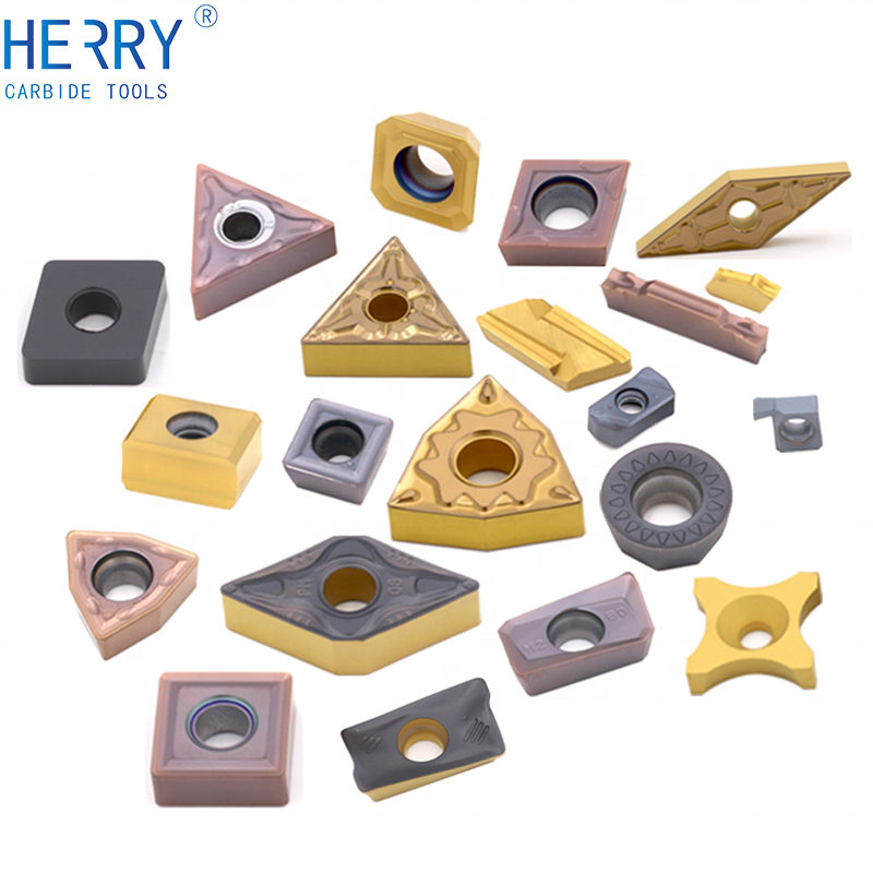
Arizona Carbide Tools Inc overview - Explorium.ai - arizona carbide
PVD (Physical Vapor Deposition): PVD coatings may have limitations in coating the sides and back of the substrate. The line-of-sight nature of PVD deposition can result in uneven coverage on complex shapes or the underside of the substrate.
PVD and CVD are both thin film coating processes, but they differ in terms of the processes they employ and the nature of the deposition. PVD relies on physical forces and does not involve chemical reactions. CVD utilizes chemical processes for thin film deposition. PVD deposition is line-of-sight, while CVD deposition is diffuse and multidirectional, resulting in differences in coating results on uneven surfaces.
CVDvsPVDinserts
Let Ms be an output, Ms0 be the nominal value, λsi (i = 1, 2, … Nt) be the constant parameter, Ti be the tolerance, and Nt is the total number of tolerances.
The nano-diamond composite coating drawing die uses cemented carbide (WC-Co) as the substrate, and uses the chemical vapor phase method ( CVD method for short ) to coat the conventional diamond and nano-diamond composite coating on the surface of the inner hole of the mold.
As we discussed in our article, What is Tolerance Analysis?, there are really four different methods of doing Stack Analysis -
Difference between pvd and cvdchemistry
CVD Diamond Cutting Tools: Superior Wear Resistance, Low Friction, High Thermal Conductivity for Non-Ferrous Materials, Ceramics, Composites Machining
It is often applied to manufactured parts in general to determine the impact of manufacturing processes on the final dimensions of those parts. Tolerances are determined by a variety of methods, from standards such as ISO or ASME, or from the use of geometric dimensioning and tolerancing (GD&T), a method of annotating and marking tolerances on parts.
Difference between pvd and cvdcar
In equation eq6, the calculation is performed based on the Normal approximation for a symmetrical Nonnormal case. It assumes there is no mean shift. A simulation method can also be used as outlined in the following case.
PVDcoating
A well performed statisitical method can reduce the manufacturing costs by accounting for acceptable levels of variation, designing what is called a Robust Design, which 'loosens' (ie. increases) the tolerances on non-critical areas where it does not affect the overall build, and focus on the critical and sensitive features of the product.
Tolerancing directly influences the cost and performance of a product. A piece of sheet metal that is quickly stamped using a stamping die is much cheaper to produce than one that needs to be machined to more precise dimensions. The same applies for plastics, composites and any given part. The tighter, as in the smaller, the tolerance, the more difficult the part is to produce, and the more expensive the part is. In the same regard, the performance of a part and product is influenced by tolerances. An automobile door will not close well if the tolerances are very large, and may have additional road noise from a poor seal. Aircraft wings may need large amounts of shims if the tolerances are incorrect in order to fit properly to the fuselage. This costs time, money and increases the weight of the aircraft, reducing its fuel efficiency.
CVD boron-doped diamond: A versatile material enabling tailored electrical conductivity, optical transparency, and exceptional thermal properties for applications in electronics, optics, sensing, and quantum technologies.
CVD (Chemical Vapor Deposition): CVD technology is capable of producing uniform thin coatings on uneven surfaces. The diffuse and multidirectional deposition allows for better coverage and conformity, even on complex shapes or the underside of the substrate.

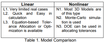
Traditional methods of tolerance analysis include 1D, 2D and 3D Tolerance Stacks, and statistical methods like Monte Carlo simulations. Tolerance Stacks calculate the accumulated variation across a set of dimensions. 1D stacks do a single directional linear stack, while 2D stacks and 3D stacks include multiple directions and influencers.
Each part is modeled using a statistical distribution for its tolerance range (variation) which are then summed using the Root Sum Squared method to predict the distribution of the assembly measurements. This process describes the variation as a distribution instead of only showing the extremes of variation, which gives more design flexibility by allowing the design and engineering team to account for varying levels of quality, instead of just 100 percent of all variation, which is statistically rare or impossible.
PVDvsCVDadvantagesanddisadvantages
CVD (Chemical Vapor Deposition): CVD deposition occurs in a flowing gaseous state. The precursors introduced into the reaction chamber undergo chemical reactions on the substrate surface, leading to the formation of a thin film. This type of deposition is diffuse and multidirectional, allowing for more uniform and conformal coatings on uneven surfaces.
PVD (Physical Vapor Deposition): PVD uses physical forces to deposit a thin film onto a substrate. The process involves gasifying a pure source material through methods like evaporation, high-power electricity, or laser ablation. The gasified material then condenses on the substrate to create the desired layer. There are no chemical reactions involved in PVD.
Disadvantages ofCVD
Statisitical Variation Analysis applies statistical controls and methods to relax component tolerances without negatively impacting product quality.
Learn about Cylindrical Resonator MPCVD Machine, the microwave plasma chemical vapor deposition method used for growing diamond gemstones and films in the jewelry and semi-conductor industries. Discover its cost-effective advantages over traditional HPHT methods.
It is important to account for manufacturing variation, as there is no such thing as perfect parts. What's more, those tolerances and variation can greatly affect production costs.
CVD diamond wire drawing die blanks: superior hardness, abrasion resistance, and applicability in wire drawing various materials. Ideal for abrasive wear machining applications like graphite processing.
The coefficient λsi in a linearized model also provides the sensitivity relationship from a tolerance Ti to a measurement Ms.
When manufactured, parts are never made to perfect specifications. Due to variation caused by material characteristics and manufacturing processes, such as stamping and machining, parts are always made larger or smaller than their nominal design. This variation is captured in design as tolerances, depicting the range of variation acceptable in the design.
CVD Diamond Coating: Superior Thermal Conductivity, Crystal Quality, and Adhesion for Cutting Tools, Friction, and Acoustic Applications
However, if we consider that tolerances are small relative to dimensions, we can approximate a non-linear relationship with a linear model. Besides the calculation advantage, the sensitivity analysis is also an important reason to have the linearized model (although, there is a coming solution in AAO Add-on for non-linear models; see the webinar at the bottom).
Difference between pvd and cvdcoating
Upgrade your coating process with PECVD coating equipment. Ideal for LED, power semiconductors, MEMS and more. Deposits high-quality solid films at low temps.
Upgrade your coating process with PECVD coating equipment. Ideal for LED, power semiconductors, MEMS and more. Deposits high-quality solid films at low temps.
Worst-case tolerance analysis is the traditional type of tolerance stackup calculation. Each tolerance is set to its largest or smallest limit in its total tolerance range. This does not consider the distribution of tolerance range, only that each tolerance stays within its expected range. This method does guarantee that that the parts will fit and function properly, regardless of actual variation. However, because this method often requires very tight individual component tolerances, as the total stack up at maximum conditions is the primary attribute used in the design, it promotes expensive manufacturing and inspection process and high scrap rates.
Looking for high-quality laboratory equipment for PVD and CVD processes? Look no further than KINTEK! With our advanced technology and expertise, we provide the best solutions for your deposition needs. Whether you need physical force-based PVD or chemical reaction-based CVD, we have the equipment to meet your requirements. Contact us today and take your research to the next level with KINTEK's cutting-edge laboratory equipment.
RF-PECVD is an acronym for "Radio Frequency Plasma-Enhanced Chemical Vapor Deposition." It deposits DLC (Diamond-like carbon film) on germanium and silicon substrates. It is utilized in the 3-12um infrared wavelength range.
915MHz MPCVD Diamond Machine and its multi-crystal effective growth, the maximum area can reach 8 inches, the maximum effective growth area of single crystal can reach 5 inches. This equipment is mainly used for the production of large-size polycrystalline diamond films, the growth of long single crystal diamonds, the low-temperature growth of high-quality graphene, and other materials that require energy provided by microwave plasma for growth.
Where sti is the adjusted sigma based on the distribution type for Ti. For example, a uniform distributed tolerance Ti will have sti 2 = (∆Ti 2 /12).

This method is often requested by customers for critical interfaces in assemblies, but as mentioned, suffers from over-tolerancing parts. The worst-case scenario rarely if ever occurs in actual production, and therefore often incurs unnecessary costs in manufacturing and quality.
The main issue in Tolerance Analysis is how to calculate the total variation from accumulating tolerances. There are two major categories in this area:
Get high-quality diamond films with our Bell-jar Resonator MPCVD machine designed for lab and diamond growth. Discover how Microwave Plasma Chemical Vapor Deposition works for growing diamonds using carbon gas and plasma.
Difference between pvd and cvdpdf
Understanding the difference between PVD (Physical Vapor Deposition) and CVD (Chemical Vapor Deposition) is crucial for anyone involved in thin film coating processes.
PVD (Physical Vapor Deposition): PVD deposition involves the vaporization of solid physical particles into a plasma, which is then deposited onto the substrate. This is a line-of-sight deposition, meaning that the deposition occurs in a specific direction. As a result, PVD may have limitations in terms of thickness and uniformity of deposition on uneven surfaces.
Introducing our inclined rotary PECVD furnace for precise thin film deposition. Enjoy automatic matching source, PID programmable temperature control, and high accuracy MFC mass flowmeter control. Built-in safety features for peace of mind.
Therefore, tolerancing and tolerance analysis are integral parts of the engineering process and product lifecycle management in order to produce high-quality products at reasonable prices.
RF-PECVD is an acronym for "Radio Frequency Plasma-Enhanced Chemical Vapor Deposition." It deposits DLC (Diamond-like carbon film) on germanium and silicon substrates. It is utilized in the 3-12um infrared wavelength range.
Get your exclusive CVD furnace with KT-CTF16 Customer Made Versatile Furnace. Customizable sliding, rotating, and tilting functions for precise reactions. Order now!
CVD (Chemical Vapor Deposition): CVD uses chemical processes to produce a thin film. During the CVD process, one or more volatile precursors are introduced into a reaction chamber along with the substrate. The precursors react or decompose on the substrate surface, forming a thin layer of coating. Chemical reactions occur in CVD.


 0086-813-8127573