
Carbide Reamers Speeds and Feeds - feeds and speeds for reamers
Largerouter bits
Metals and alloys are some of the most widely used materials in manufacturing today due to their high strength, reliable properties, and processability. Metals and alloys are commonly used in construction, medical devices, small part manufacturing, and many other applications. Our NAT lab can perform alloy phase identification and element distribution analysis using scanning electron microscopy (SEM) and x-ray energy dispersive spectroscopy (EDS). We have an STA 449 F3 Jupiter Thermal Analyzer, which can perform differential scanning calorimetry (DSC) and thermogravimetric analysis (TGA) simultaneously. The Jupiter Thermal Analyzer can precisely measure the temperature of a phase transformation or decomposition up to 1650 °C.
ProfileRouter bits
Have some unknown samples? We can help you to determine what they are and where they came from. X-ray Energy Dispersive Spectroscopy (EDS) is a semi-quantitative x-ray technique that can identify and measure chemical composition in SEM analysis. Figure 1 shows the principle of EDS. The SEM focuses an electron beam on the sample surface. The electrons knock core-shell electrons out of atoms inside the sample. To fill this vacancy, a higher energy electron from the atom will fall down to take its place, and the difference in energy between the two states is emitted as an x-ray. The generated x-rays possess energies unique to the element which are dependent upon the atomic number (Z) and the orbital transition involved. Measuring the spectrum of emitted x-ray allows for chemical characterization of the sample.
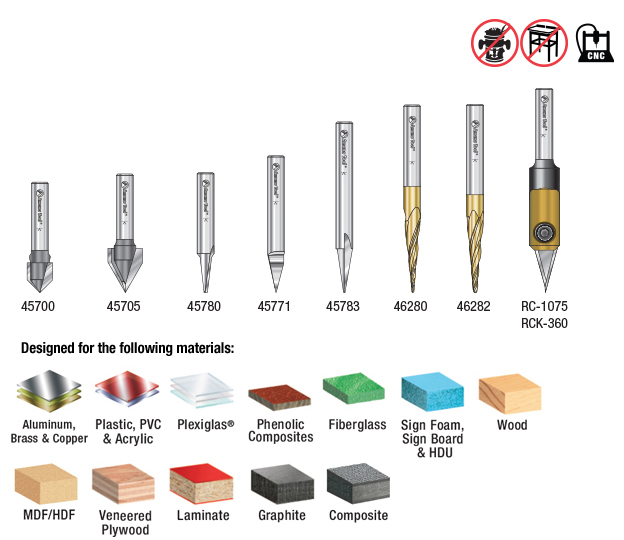
Excellent for a wide-range of signmaking lettering and engraving tasks this set is specially designed for creating signs and other CNC projects in a variety of materials. Each router bit is manufactured from Amana’s exclusive grade carbide according to stringent quality standards.
CanCam’s slogan is ‘Up in Class, Down in Price’ provide high quality CNC routers and CNC laser cutters and engravers built with the best components that provide reliable, accurate, and quick fabrication.
1 8 in shank router bitshome depot
At Ebatco we offer technical expertise, state of the art instruments, market-competitive service charge rates, a quick turn around and guaranteed satisfaction! Please contact us with any questions that you may have.
Backscatter electron image of a Zinc-Aluminum alloy. The brighter regions are the Zinc rich phase, the dull gray regions are the Aluminum rich phase, and the black regions are voids within the casting.
TungstenRouter Bits
Lee valleyrouter bits
Through EDS, we found that this sample is mainly composed of Zn with Al as an alloying element. The elemental concentrations were calculated by difference, and the K lines were selected to do the quantitative analysis. Table 1 lists the individual and average EDS results. The average concentrations of Zn and Al are 93.8 and 6.2 wt% respectively, which is a common composition for zinc die castings. Zn alloys have excellent finishing characteristics for plating, and chromate treatments. It is low cost, has excellent thin wall capabilities, and possesses high strength and hardness.
EDS can also do high resolution composite element mapping. Through the element map, we can see a detailed overview of where the different elements are located. Figure 3 clearly indicates that there were three layers of coating on the emblem. The innermost layer in direct contact with the Zn-Al substrate was identified as Cu. The middle layer was Ni, and the outermost layer was Cr. This coating was likely prepared by an electroplating process where the Cu layer facilitated the formation of a good Ni coating. This is a common processing step for electroplating Ni onto cast metal parts. The thicknesses of the Ni and Cr coatings are approximately 20 and 2 µm, respectively.
this project, an automotive emblem of unknown composition was analyzed by SEM/EDS. EDS can measure the composition at a single point, along a line, or map an area. In this case, the chemical composition was analyzed by EDS area scanning following ASTM E1508 – 12a using an accelerating voltage of 15 kV, take-off angle of 35º, and sample tilt of 0º. The test was performed using a standardless method with P/B-ZAF matrix correction. Figure 2 shows a typical microstructure and the resulting EDS spectrum. Five randomly selected areas at 200X magnification were analyzed by EDS.


 0086-813-8127573