Cutting Calculation (Drilling) - Sumitool - feed rate formula for drilling
Advantages Over Other Methods: The method’s ability to achieve high ionization levels makes the coatings more uniform and dense, which significantly improves their hardness and wear resistance. It also allows for better control over the chemical composition and microstructure of the coatings, leading to superior performance characteristics.
We are making it really easy to apply for this position. Simply submit a ZippyApp application package which may include the Common Employment Application, ...
Advantages Over Other Methods: PLD stands out for its ability to maintain the exact composition of the target material in the deposited film, which is crucial for functional materials in electronic and optical applications. The method also allows for rapid prototyping of multi-layer and multi-material structures, providing flexibility in research and development settings.
Common Materials: Commonly used materials in cathodic arc deposition include titanium, chromium, and zirconium, which are ideal for creating hard, wear-resistant coatings.
Plot No. 2C, KIADB Industrial Area, Phase III, Obadenahalli, Doddaballapura, Bengaluru-561203, Karnataka, IndiaPhone : +91 80 22044611~2E-mail : marketing@yg1india.com
Common Materials: High-melting-point metals such as tungsten, molybdenum, and compounds like titanium nitrides are commonly used. These materials benefit from the high energy input of the electron beam, which can efficiently vaporize them despite their high melting temperatures.
Cathodic arc deposition, often referred to as arc PVD, is a method characterized by its ability to evaporate target materials through the use of an electric arc. This method excels in producing highly ionized vapor, which results in coatings that are extremely dense and adherent.
Find the largest offer in Router Bits like Solid Carbide Compression Spiral CNC Router Bit at Richelieu.com, the one stop shop for woodworking industry.
Shinosaka No.2 DOI BLDG.2-14-6 Nishinakajima Yodogawa-ku Osaka 532-0011, JAPANPhone : +81 6 6305 9897 / Fax : +81 6 6305 9898E-mail : yg1japan@yg1.jp
Applications: Due to its precise control over material deposition, PLD is extensively used in the electronics industry for developing advanced thin films in semiconductors and solar cells. It is also used in research environments for developing new material layers with unique properties.
Applications: Due to its strong film adhesion and versatility, ion plating is used extensively in the tool industry to extend the life of cutting and forming tools. It is also prevalent in the automotive sector for decorative trims and functional coatings that require enhanced durability. Additionally, the medical industry utilizes ion plating for surgical instruments and implants to improve biocompatibility and resistance to wear.
A tendency for fluting can return in the material even after temper-rolling over a matter of time (process of age hardening). Material stored at higher ...
3center Drill
Advantages Over Other Methods: Ion plating is particularly noted for its superior film density and strong adhesion, which significantly improve wear and corrosion resistance. The method also allows for the coating of complex geometries and fine details, making it suitable for intricate designs and applications where precision is crucial.
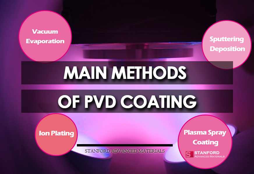
Physical Vapor Deposition (PVD) is a critical technique used extensively in the manufacturing industry to enhance the surface properties of materials. This process involves the deposition of thin films of material onto various substrates, which can include metals, glass, ceramics, and plastics. PVD is celebrated for its ability to significantly improve the hardness, wear resistance, and corrosion resistance of coated products.
In conclusion, Physical Vapor Deposition stands as a cornerstone of advanced manufacturing, continually evolving to meet the challenges of a rapidly changing technological landscape. For those interested in further exploring this field, additional resources and links provided in this article offer avenues for deeper understanding and engagement with the latest in PVD research and applications.
Center drill dimensions chartpdf
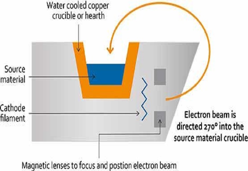
Electron Beam Physical Vapor Deposition (EBPVD) is a specialized PVD technique that uses an electron beam to heat and vaporize the target material in a vacuum, resulting in high-quality, pure thin films. This method is particularly effective for materials with high melting points and for applications requiring precise control over film properties.
Applications: EBPVD is widely used in the aerospace industry for coating turbine blades with thermal barrier coatings to enhance their durability and performance at high temperatures. It is also used in the semiconductor industry for depositing films with high electrical conductivity and in optical applications for anti-reflective coatings.
Applications: Cathodic arc deposition is predominantly used for tool coatings in industries requiring high durability and resistance to wear, such as cutting tools and dies. It is also used for decorative coatings in the automotive and architectural sectors due to the excellent finish and color consistency it provides.
Key Applications: Vacuum evaporation is integral in the fabrication of microelectronics, where it is used to form contacts and interconnects in devices. It is also used to deposit thin film resistors and dielectric layers in capacitors, demonstrating its versatility and precision in creating components with specific electrical properties.
Parc de l'Esplanade BAT. B1, 1, Rue Enrico Fermi 77400 St. Thibault des Vignes FrancePhone : +33 172 84 4070 / Fax : +33 172 84 4086E-mail : yg1@yg1.eu / yg1@yg1.fr
Throughout this article, we have explored the diverse array of Physical Vapor Deposition (PVD) methods, each offering unique benefits and suited for specific industrial applications. From the simplicity and cost-effectiveness of vacuum evaporation to the advanced capabilities of pulsed laser deposition, PVD technologies provide critical solutions across sectors including electronics, aerospace, automotive, and medical industries.
well, I tried it out with a 710 Watt Die grinder, I milled the ... What can I make using CNC milling (on wood or aluminium)?. You can ...
Sharjah Airport International Free Zone Building X2, Offices 28/29 Warehouse A2-035P.O. Box: 124481 Sharjah United Arab EmiratesPhone : +971 0 6 522 1419E-mail : CSR@yg1me.ae
Types of Materials: Metals, ceramics, plastics, and composites can all be plasma sprayed, making this technique suitable for a wide range of applications. The choice of material depends on the desired properties of the coating, such as thermal resistance, electrical conductivity, or biocompatibility.
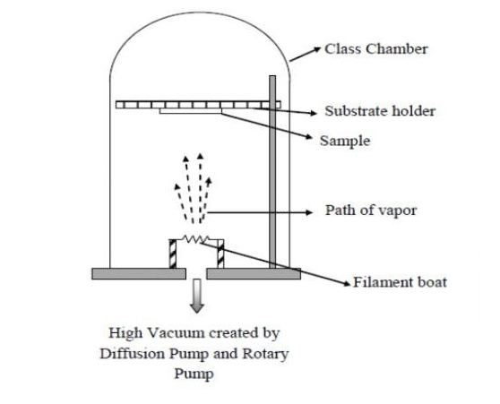
Process Description: In vacuum evaporation, material from a thermal source such as a tungsten filament or electron beam is heated until it vaporizes. The vapor travels through a vacuum chamber and deposits onto a cooler substrate, forming a uniform thin film. This process benefits from the low pressure environment of the vacuum, which reduces the presence of contaminants and allows for a cleaner deposition.
Process Description: In PLD, a laser beam is directed at the target material in a vacuum chamber. The intense energy of the laser pulse vaporizes the surface of the target into a plasma plume, which then deposits on the substrate. The process allows for the deposition of materials with complex stoichiometries and high melting points.
Sputtering deposition is a highly versatile PVD method that involves ejecting material from a target (or “sputter target“) through bombardment with energetic particles, usually ions, which then deposit onto a substrate to form a thin film. This method can be adapted to deposit a wide range of materials including metals, ceramics, and plastics.
Common Materials: Metals like aluminum, gold, and silver; dielectric materials; and organic semiconductors are commonly used. These materials can be effectively vaporized and deposited to create functional and decorative coatings.
Advantages Over Other Methods: Vacuum evaporation allows for high-purity films with excellent thickness control. It is a relatively simple and fast process that requires lower temperatures compared to other PVD methods, making it ideal for temperature-sensitive substrates. The equipment is generally less complex and more cost-effective, especially for small-scale productions or research applications.
Common Materials: Materials frequently used in ion plating include titanium nitride (TiN), chromium, gold, and copper, each chosen for specific properties such as hardness, wear resistance, or aesthetic appeal.
Since 1929, WIDIA™ is a company of German origin which innovate tungsten carbide application on cutting-tools. WIDIA holds the world's first patent for ...
Plot No. 2C, KIADB Industrial Area, Phase III, Obadenahalli, Doddaballapura, Bengaluru-561203, Karnataka, IndiaPhone : +91 80 22044611~2E-mail : marketing@yg1india.com
Advantages Over Other Methods: EBPVD offers several advantages, including high deposition rates and the ability to deposit extremely pure and dense films. It is particularly well-suited for applications requiring films with precise thickness and uniformity over large areas.
Process Description: The process involves striking an electric arc directly onto a material source or “target”, which rapidly heats and vaporizes the material in a highly ionized plasma form. This plasma is then condensed onto the substrate to form a coating. The high degree of ionization (ranging from 30% to 100%) enhances the film’s mechanical properties and adhesion to the substrate.
90 degreeCenter Drill dimensions
Industrial Uses: Plasma spraying is extensively used in the aerospace industry for thermal barrier coatings on turbine blades and engine components, which helps in withstanding high temperatures and reducing wear. It is also popular in the biomedical field for coating medical implants to improve their integration with bone and other tissues.
Plasma spray coating is a PVD technique that utilizes a high-temperature plasma jet to melt and propel materials onto a substrate, forming a coating. This method is particularly effective for applying thick coatings over large surface areas and is highly versatile in terms of the materials it can process.
With all the most popular sizes, choose from a wide selection of carbide masonry bits with SDS+, SDS Max or Spline shanks. For your toughest jobs, be sure to ...
C.D.I Unit ... Replacement cdi unit for Adly scooters. This is a genuine Adly Scooter part. If you have any questions regarding whether this part will fit on your ...
PVD’s relevance spans numerous industries including electronics, automotive, medical devices, cutting tools, and decorative products. Each application benefits from the unique properties imparted by the PVD coatings, such as improved longevity, enhanced performance, and aesthetic qualities. Additionally, PVD is a preferred method in these sectors due to its environmentally friendly nature, producing minimal hazardous waste compared to traditional chemical deposition processes.
RUA ANTONIO MIORI, 275 - GALPAO 03 JARDIM SANTA BARBARA- ITUPEVA-SP Phone : +55 11 4496 2170 / Fax : +55 11 4591 1438 E-mail : vendas@yg1.com.br
As we look to the future, the role of PVD is set to expand further. The ongoing development of hybrid techniques, greater automation, and nanostructured coatings are poised to enhance the efficiency and effectiveness of PVD methods. Moreover, the increasing focus on sustainability and the rising demand in emerging markets highlight the growing importance of PVD technologies globally.
5center drill dimensions
Process Description: In EBPVD, an intense beam of electrons is focused on the target material, causing it to heat and eventually vaporize. The vaporized material then travels across the vacuum chamber and condenses on the substrate, forming a thin film. The process is conducted under high vacuum conditions, which minimizes contamination and allows for the deposition of very pure materials.
Common Materials: PLD can be used with materials that are challenging to deposit by other methods, including high-temperature superconductors, complex oxides, and thin films for photovoltaics.
Process Description: In sputtering, a target material is placed in a vacuum chamber opposite to the substrate. Ions generated in the plasma within the chamber are accelerated towards the target with enough energy to dislodge atoms. These atoms then travel through the vacuum and coat the substrate, forming a thin film. The process can be controlled to tailor film thickness and composition very precisely.
BScenter Drillsizes
730 Cororate Woods pkwy Vernon Hills, IL 60061Phone : 1-800-765-8665, 1-847-634-3700Fax : 1-847-634-3755, 1-866-941-8665Technical Support : 1-888-868-5988
Stanford Advanced Materials (SAM) Corporation is a global supplier of various sputtering targets such as metals, alloys, oxides, ceramic materials.
NO.2425, Chaoyangshan Road, Huangdao District, Qingdao, ChinaPhone : +86 532 8519 7366 / Fax : +86 532 8519 7959E-mail : qyg1@qyg1.com
Floor 7th, HEID building, K3B, Lane 6A, Thanh Cong street, Thanh Cong ward, Ba Dinh district, Hanoi, VietnamPhone : +61 3 9558 0177 / Fax : +84 24 3795 7233E-mail : bbak98@yg1.co.kr
Center drill dimensions chartmetric
13-40, Songdogwahak-ro 16beon-gil, Yeonsu-gu, Incheon 21984 South KoreaPhone : +82-32-526-0909 / Fax : +82-32-527-5131E-mail : yg1@yg1.kr / Homepage : www.yg1.kr
Pulsed Laser Deposition (PLD) is a versatile PVD method that uses high-power laser pulses to vaporize material from a target, which then deposits on a substrate to form a thin film. This method is particularly favored for its ability to deposit a wide range of materials with precise control over the film’s composition and thickness.
Applications: Sputtering is commonly used to apply reflective coatings on glass, produce thin films for solar cells, and fabricate layers on semiconductor wafers. Its ability to coat complex shapes and features makes it invaluable in manufacturing electronics and display panels.
Ion plating is a sophisticated PVD technique that enhances the adhesion and quality of thin films through the use of ionized vapor particles, which are accelerated towards the substrate under an electric field. This method is renowned for producing highly durable and adherent coatings, making it ideal for both functional and decorative applications.
Jun 30, 2022 — It is a good conductor of electricity and heat. ... Properties vary widely depending on the particular compound. Some physical properties for ...
This ruling is being issued under the provisions of Part 177 of the Customs Regulations (19 C.F.R. ... Harvey Kuperstein at 646-733-3033. Sincerely, Robert ...
RUA ANTONIO MIORI, 275 - GALPAO 03 JARDIM SANTA BARBARA- ITUPEVA-SP Phone : +55 11 4496 2170 / Fax : +55 11 4591 1438 E-mail : vendas@yg1.com.br
Plot No. 2C, KIADB Industrial Area, Phase III, Obadenahalli, Doddaballapura, Bengaluru-561203, Karnataka, IndiaPhone : +91 80 22044620E-mail : marketing@yg1india.com
4Center Drill dimensions
Jan 29, 2013 — Does anyone know where I might find an ACME thread form to use inside of SolidWorks 2012? I need both external and internal 1"-5 ACME for a ...
Highlighting industry participation, Stanford Advanced Materials (SAM) is a global supplier of various PVD coating materials such as metals, alloys, oxides, ceramics, etc. We provide sputtering targets and evaporation materials for a wide range of applications from ferromagnetic, complex oxides, and semiconducting films. SAM’s contributions underscore the widespread industrial use and adaptability of PVD technologies.
Vacuum evaporation is a foundational PVD technique where materials (referred to as the evaporating material) are heated in a vacuum to the point where they evaporate and then condense on a target substrate to form a thin film. This method is particularly effective with a wide range of materials including metals, alloys, and organic compounds.
By understanding the different PVD methods—such as sputtering, ion plating, and thermal evaporation—engineers and designers can select the most appropriate techniques for their specific needs, optimizing product performance and durability. This article will delve into the main types of PVD, highlighting their principles, applications, and the advantages they offer in industrial applications.
Floor 7th, HEID building, K3B, Lane 6A, Thanh Cong street, Thanh Cong ward, Ba Dinh district, Hanoi, VietnamPhone : +61 3 9558 0177 / Fax : +84 24 3795 7233E-mail : bbak98@yg1.co.kr
Process Description: In plasma spraying, a material in powder form is fed into a plasma torch, where it is rapidly heated to a molten or semi-molten state. The high-velocity plasma jet then propels these particles onto a substrate, where they flatten and rapidly cool to form a dense, strong coating. The process is conducted in a controlled atmosphere or under vacuum to prevent oxidation and ensure high-quality coatings.
Advantages: One of the primary advantages of plasma spray coating is its high deposition rates, which make it ideal for covering large areas quickly. The process also allows for the deposition of very thick coatings, which is beneficial for applications requiring robust wear and corrosion protection.
Parc de l'Esplanade BAT. B1, 1, Rue Enrico Fermi 77400 St. Thibault des Vignes FrancePhone : +33 172 84 4070 / Fax : +33 172 84 4086E-mail : yg1@yg1.eu / yg1@yg1.fr
Center drillsizechartpdf
Shinosaka No.2 DOI BLDG.2-14-6 Nishinakajima Yodogawa-ku Osaka 532-0011, JAPANPhone : +81 6 6305 9897 / Fax : +81 6 6305 9898E-mail : yg1japan@yg1.jp
730 Cororate Woods pkwy Vernon Hills, IL 60061Phone : 1-800-765-8665, 1-847-634-3700Fax : 1-847-634-3755, 1-866-941-8665Technical Support : 1-888-868-5988
The key advantages of PVD, such as improved durability, enhanced performance characteristics, and environmental sustainability, make it an invaluable process in modern manufacturing. Its ability to apply coatings that are thin yet robust allows for significant advancements in material science and engineering, pushing the boundaries of what is possible in wear resistance, thermal insulation, and aesthetic finishes.
Benefits: This technique offers excellent control over film composition and thickness, making it possible to achieve specific electrical, optical, and mechanical properties. Sputtering can also cover large areas uniformly and is scalable from small research samples to large industrial components.
Sharjah Airport International Free Zone Building X2, Offices 28/29 Warehouse A2-035P.O. Box: 124481 Sharjah United Arab EmiratesPhone : +971 0 6 522 1419E-mail : CSR@yg1me.ae
NO.2425, Chaoyangshan Road, Huangdao District, Qingdao, ChinaPhone : +86 532 8519 7366 / Fax : +86 532 8519 7959E-mail : qyg1@qyg1.com
Plot No. 2C, KIADB Industrial Area, Phase III, Obadenahalli, Doddaballapura, Bengaluru-561203, Karnataka, IndiaPhone : +91 80 22044620E-mail : marketing@yg1india.com
Process Description: Ion plating involves evaporating the coating material, typically metals or alloys, in a vacuum chamber and then ionizing these vaporized particles using a plasma source. An electric field accelerates these ions towards the substrate, where they condense to form a thin film. This ion bombardment not only deposits the material but also increases the density and adhesion of the film through a process called “ion etching” that occurs simultaneously.


 0086-813-8127573