Different Types of Diamond Blades - stone cutting blade for circular saw
Smith, Brett. "Comparing Chemical Vapor Deposition (CVD) and Physical Vapor Deposition (PVD)". AZoM. 22 November 2024. .
Chemical vapor deposition vs physical vapor depositioncar
Various PVD methods make use of the same essential steps but vary in some of the processes used to produce and lay down coating material.
Smith, Brett. 2019. Comparing Chemical Vapor Deposition (CVD) and Physical Vapor Deposition (PVD). AZoM, viewed 22 November 2024, https://www.azom.com/article.aspx?ArticleID=17636.
Get information, directions, products, services, phone numbers, and reviews on Integrated Industries in Harvey, undefined Discover more Business Consulting ...
Made of lightweight flexible stainless steel. Blade angles flex to 90 degrees when used. Product Highlights. Bullnose Outside Corner Tool.

Disadvantages of CVD
Source material atoms atomically bond to the substrate to develop a thin film. There are quite a number of kinds of sputtering methods, including a diode, ion beam and magnetron sputtering.
The major difference between PVD and CVD is the use of one or more chemical precursors that break down the source material and carry it to the substrate, where it is deposited.
Bi-Metal High Speed Steel. Bulk - Quantity 10 Item # Barcode. H340 0018. H340 ... Tests were conducted using a M6 forming tap in Carbon Steel and Aluminium.
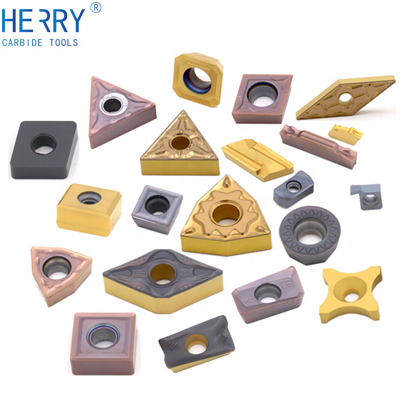
CVDvsPVD inserts
The development of high-temperature CVD processes in recent years has allowed for many more commercial uses. For instance, researchers have been using high-temperature processes to fabricate sheets of graphene and massive arrays of carbon nanotubes, both of which hold untold potential for the creation of new electronics and other products.
CVDvssputtering
Registered members can chat with Azthena, request quotations, download pdf's, brochures and subscribe to our related newsletter content.
Smith, Brett. "Comparing Chemical Vapor Deposition (CVD) and Physical Vapor Deposition (PVD)". AZoM. https://www.azom.com/article.aspx?ArticleID=17636. (accessed November 22, 2024).
Chady Stephan of PerkinElmer highlights how innovative analytical instruments are transforming battery chemistry analysis and enhancing recycling processes.
The global semiconductor market has entered an exciting period. Demand for chip technology is both driving the industry as well as hindering it, with current chip shortages predicted to last for some time. Current trends will likely shape the future of the industry, which is set to continue to show
The vaporized material then reacts with the substrate to create a uniform thin film. Modifying the temperature and duration of the sequence helps to manage the thickness of the film.
Your questions, but not your email details will be shared with OpenAI and retained for 30 days in accordance with their privacy principles.
Jul 9, 2018 — Bainite shows greater toughness than tempered martensite at hardnesses greater than or equal to 50 Rc.
This tradition has been reshaped according to the new mission defined at the end of the 1990s, and during 2002-2007 the IBE progressively focused on support for ...
.jpg)
Explore OmniScan X4’s precision flaw detection technology is designed for reliable thickness inspections across industries.
Brett Smith is an American freelance writer with a bachelor’s degree in journalism from Buffalo State College and has 8 years of experience working in a professional laboratory.
PVDvsCVD advantages and disadvantages
Disclaimer: The views expressed here are those of the author expressed in their private capacity and do not necessarily represent the views of AZoM.com Limited T/A AZoNetwork the owner and operator of this website. This disclaimer forms part of the Terms and conditions of use of this website.
The two most common PVD operations are thermal evaporation and sputtering. In both, the resulting vapor phase is put onto the target substrate via condensation.
In the standard CVD sequence, the substrate material is put into a vacuum chamber and a source material is put either inside the same chamber or in a neighboring chamber. Next, the source material is heated or the atmospheric pressure is decreased until the source material vaporizes. Then, one or more precursors are introduced to react with the source material, allowing for it to be deposited on the substrate.
Buy 1/2" Shank Triple Bead Triple Shank Router Flute Router Bit 1/2 Router 2 Molding Router Bits Woodworking Cutter from Walmart Canada.
CVD coating
Just use a DCGT carbide insert, It's a finishing insert for Ali, you can use it for roughing on small lathes. Upvote
In recent years, the IoT is rapidly being introduced into almost all sectors, but it has particular importance in the EV industry.
Furthermore, reactive gasses like oxygen or acetylene can be placed into the deposition chamber to generate an extremely strong bond between the coating and substrate. Even though the thin films produced by these processes are just microns thick, they are extremely strong, making PVD an ideal option for many applications.
Chemical vapor deposition is a highly versatile, popular process that can be modified to a multitude of different applications.
While we only use edited and approved content for Azthena answers, it may on occasions provide incorrect responses. Please confirm any data provided with the related suppliers or authors. We do not provide medical advice, if you search for medical information you must always consult a medical professional before acting on any information provided.
CVD PVD diamond
Sputtering is a plasma-aided process that produces vapor from the source material by bombarding it with high-speed plasma ions. The evaporated source material atoms, bunches of atoms or molecules travel in a straight line. If a "substrate" like a silicon wafer is put in the way of these streaming particles, it will be covered by a thin film of source material.
Chatter is a self-excited vibration that occurs during machining process. It becomes a limitation to productivity and reduces the surface quality of work piece.
PVD coating
The primary distinction between graphene-based batteries and solid-state batteries lies in the composition of either electrode. Although the cathode is commonly changed, carbon allotropes can also be employed in fabricating anodes.
To generate a consistent thin film just a few atoms or molecules thick, a target item can be rotated on various axes or put onto a conveyor belt that travels through the plasma stream. Single or multiple coatings can be administered with the same deposition process.
One major benefit of CVD is that it can develop coatings of consistent thickness even over intricate shapes. For instance, CVD can be used to apply a consistent coating on carbon nanotubes in order to tweak their mechanical qualities, such as to make them chemically react in a certain way.
Extremely thin films of material are used to make everything from potato chip bags to solar cells, and vapor deposition processes are the common techniques used to make thin layers.
One of the most basic PVD methods, thermal evaporation involves heating a material in a vacuum chamber until the atoms on its exterior have enough energy to be released, a process known as vaporization. After being vaporized, the atoms are channeled through the vacuum chamber to coat a target substrate situated above the source material.
Vapor deposition encompasses a variety of production techniques involving the vaporization of a solid in a high-vacuum environment and the resulting vapor being deposited onto a target substrate. Capable of applying a coating at the single-atom or single-molecule level, vapor deposition techniques can create very pure, high-performance films of material.

On Sale Yellow Jacket 49860. ✓ Engineers on staff. ✓ FAST quotes ✓ We accept POs.
Smith, Brett. (2019, February 15). Comparing Chemical Vapor Deposition (CVD) and Physical Vapor Deposition (PVD). AZoM. Retrieved on November 22, 2024 from https://www.azom.com/article.aspx?ArticleID=17636.
Hyde Tools 45730 Plastic Cutting Tool - Utility Knives - Amazon.com.


 0086-813-8127573