European Strategic Programme on Research in ... - esprit technologies
2.Look for tools with built-in pilots: Tools with pilots or guides can help to maintain concentricity and alignment with the pilot hole.
By the end of this guide, you will have a solid understanding of spotface and counterbore holes and how to effectively incorporate them into your machining processes.
1.Identify the location: Determine where the spotface needs to be created based on the fastener's location and the workpiece's design.
A: Spotface holes are shallow, providing a flat surface for fasteners to sit flush. Counterbore holes are deeper, allowing fastener heads to be recessed below the surface. Spotfaces have a simple cylindrical shape, while counterbores have a stepped profile.
Selecting the right tools for counterbore and spotface machining is essential for achieving the desired results. Here are some tips to keep in mind:
A vacuum environment plays a crucial role in the PVD coating process. First, it removes air and other gases from the chamber, preventing unwanted reactions between these gases and the source material or the substrate. This is particularly important for the deposition of reactive materials, such as metals, that can oxidize in the presence of oxygen.
1.Consider the hole size and depth: Choose tools that match the required diameter and depth of the feature. For counterbores, ensure that the tool can accommodate the height of the fastener head.
The automotive industry also heavily relies on spotface and counterbore holes for assembling engines, suspension systems, and other critical components. These features ensure proper alignment, secure fastening, and a clean, professional appearance in the final product.
A: Converting a counterbore hole to a spotface hole is possible by machining the hole to a shallower depth. However, converting a spotface to a counterbore may be more challenging, as it requires deepening the hole. It's best to design and machine the correct feature from the start.
Compared to spotface holes, counterbore holes have a deeper recess and a more pronounced step between the two diameters. While spotfaces are primarily used to create a flat seating surface, counterbores are designed to hide the fastener head within the workpiece.
An aerospace manufacturer was experiencing issues with the assembly of a critical component due to misaligned fasteners. By incorporating spotface holes in the design, they were able to create a flat, even seating surface for the fasteners, ensuring proper alignment and a secure connection. This simple change eliminated the assembly issues and improved the overall quality of the final product.
3.Select the spotfacing tool: Choose a spotfacing tool with the appropriate diameter and depth capacity for the desired spotface size.
Counterbore tools often resemble drill bits or end mills, with a pilot tip that fits into the pre-drilled hole. The cutting edges are designed to create a flat-bottomed hole with straight walls. Some counterbore tools have adjustable depths to accommodate different fastener head heights.
● Automotive: In engine blocks, counterbores are used to hide the heads of bolts that secure the cylinder head, creating a smooth surface for the gasket to seal against.
● Bearing surfaces: Spotfaces can provide a flat, perpendicular surface for bearings to rest against, reducing wear and ensuring smooth rotation.
Sputtering is widely used in the semiconductor industry due to its versatility and precision. It can deposit a wide range of materials, including metals, alloys, and compounds, onto various types of substrates. It also allows for precise control over the composition and coating thickness of the film, which is critical for the fabrication of semiconductor devices.
Spotface and counterbore holes share some similarities, but they also have distinct differences. Both are cylindrical recesses machined into a workpiece, typically around an existing hole. However, the depth, shape, and callout symbols set them apart.
Spotfaces are characterized by their shallow depth, usually just enough to create a flat surface. They have a circular shape and a diameter that matches the size of the fastener's head or mating component. The bottom of a spotface is perpendicular to the axis of the hole, ensuring proper alignment and contact with the fastener.
5.Communicate surface finish needs: If a particular surface finish is required for the counterbore or spotface, make sure to specify this on the drawing or in the design documentation.
Among these techniques, drilling is particularly important for creating holes in machined parts. Holes serve various purposes, such as allowing for the passage of fluids, providing clearance for fasteners, and enabling the assembly of multiple components.
PVDcolorcoating
PVD coating is also used to deposit dielectric layers in ICs. These are insulating layers that separate the conductive paths and prevent electrical shorting. Commonly used dielectric materials include silicon dioxide and silicon nitride, which can be deposited using PVD techniques.
● Fastener seating: Spotfaces provide a flat, even surface for fasteners to sit against, ensuring proper alignment and a secure connection.
3.Assembly constraints: Consider the space available for the fastener installation. Counterbores require more depth and may not be suitable for thin workpieces or tight spaces.
Despite these challenges, PVD coating remains a cornerstone of semiconductor manufacturing, with ongoing research and development aimed at improving its capabilities and expanding its applications. As the demand for smaller, faster, and more energy-efficient semiconductor devices continues to grow, so too does the importance of PVD coating in enabling these advancements.
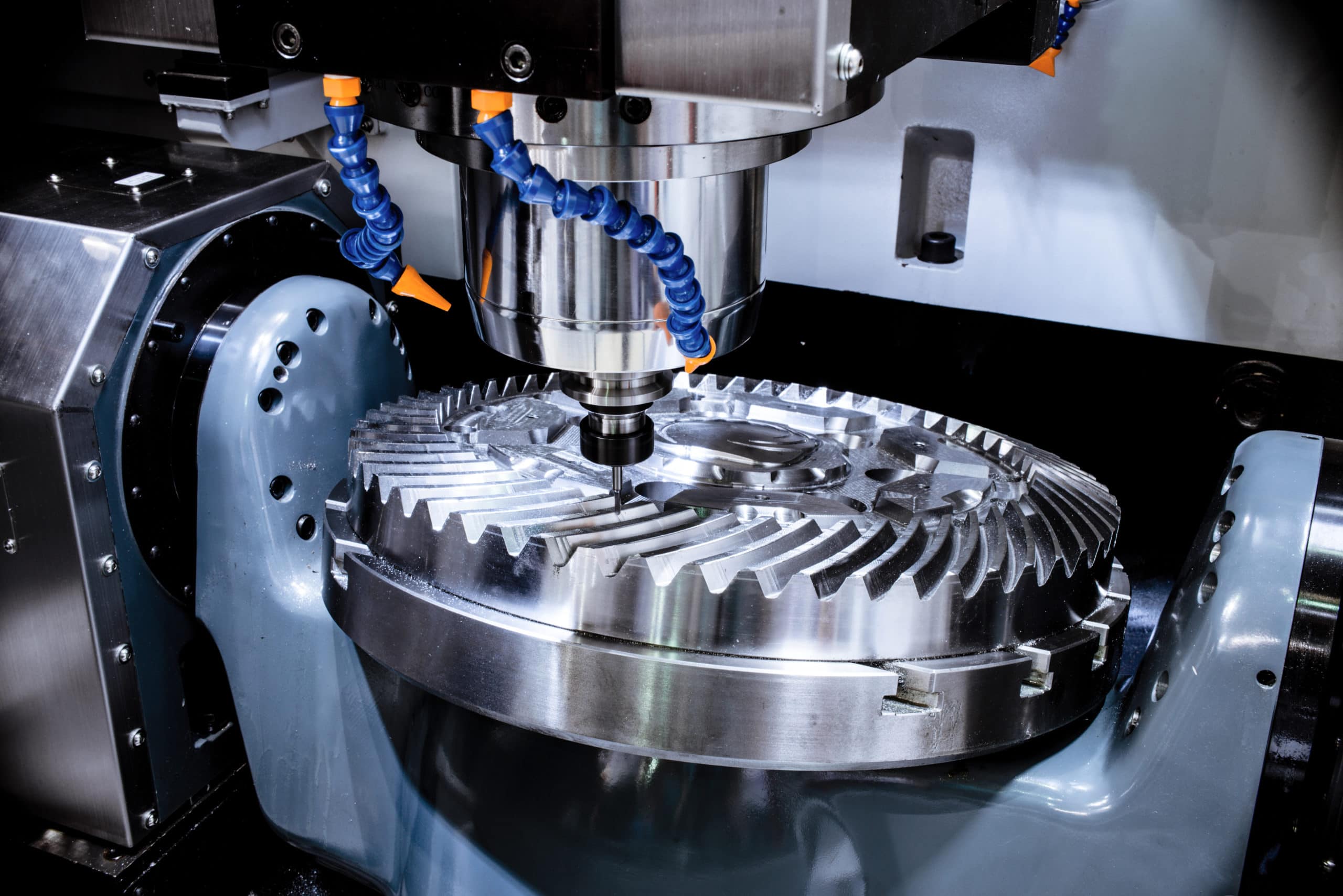
Machining is a crucial process in manufacturing that involves shaping and finishing raw materials into precise parts and components. This process is essential for creating high-quality products in various industries, from automotive and aerospace to medical and consumer goods. Some key machining techniques include:
A: The two primary types of PVD processes used in the semiconductor industry are sputtering and evaporation. Both processes involve the vaporization of the source material, but they differ in the method used to vaporize the material and the characteristics of the resulting film.
3.Enhancing assembly: Counterbores can help align and locate mating parts during assembly, making the process easier and more accurate.
Evaporation is another PVD process used in the semiconductor industry. It involves heating the source material to high temperatures, causing it to vaporize. The vaporized atoms or molecules then travel across the vacuum chamber and condense on the substrate, forming a thin film. Evaporation is typically used for the deposition of pure metals, as it can achieve high deposition rates and high-purity films.
2.Provide detailed dimensions: Include the diameter, depth, and any other relevant dimensions for the counterbore or spotface. For counterbores, specify the fastener head height to ensure proper fit.
In contrast, spotfaces have a shallower depth, usually just enough to create a flat, even surface for the fastener head. The depth of a spotface is typically less than 5 mm, as its primary purpose is to provide a smooth seating surface rather than fully concealing the fastener head.
In the semiconductor industry, a variety of materials can be deposited using PVD coating techniques. These materials serve different purposes in the fabrication of semiconductor devices, such as forming conductive layers, barriers, or insulating layers. The choice of material depends on factors such as the desired electrical, thermal, and mechanical properties of the film, as well as its compatibility with the underlying substrate and other materials in the device.
In counterbores, the surface finish of the side walls is less critical, as they primarily serve to accommodate the fastener head. The bottom surface of a counterbore, where the fastener head rests, still requires a smooth finish for proper seating.
Machining processes and tools used for creating spotfaces and counterbores can impact the achieved surface finish. Proper tool selection, cutting parameters, and machining techniques are essential to obtain the desired surface quality.
Second, a vacuum environment facilitates the vaporization of the source material and the migration of the vaporized atoms or molecules toward the substrate. In a vacuum, the mean free path of the atoms or molecules (the average distance they can travel without colliding with other particles) is significantly increased. This allows the atoms or molecules to travel directly from the source to the substrate, resulting in a uniform and high-quality film. [2]
Another critical stage in IC fabrication where PVD is used is the formation of interconnects. These are conductive paths that link the various components of the IC, enabling electrical signals to travel across the device. Interconnects are typically formed of copper or aluminum, which are deposited using PVD techniques such as sputtering or evaporation. A barrier layer of a coating material like titanium or tantalum is often deposited prior to the metal layer to prevent diffusion between the metal and the underlying silicon.
Surface finish of the side walls is less critical, but the bottom surface still requires a smooth finish for proper seating
4.Consider the surface finish requirements: Some tools are designed to produce a finer surface finish than others. Choose tools with the appropriate geometry and edge preparation for your specific needs.
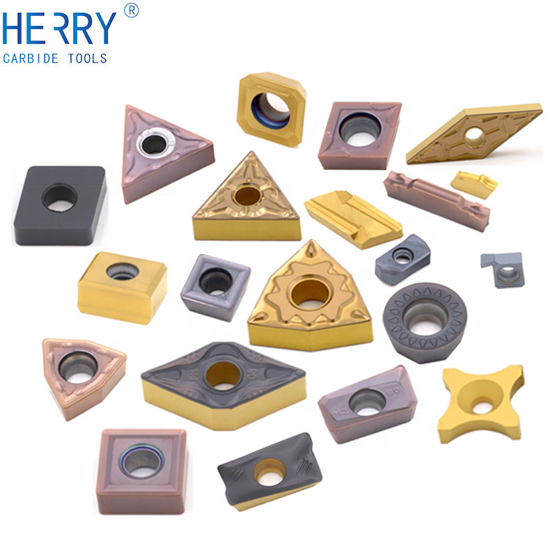
Specialized tools are available for both counterbore and spotface machining operations. These tools come in various geometries and sizes to accommodate different hole diameters and depths.
2.Consider the materials being used. Different materials may require different machining processes or feature dimensions to achieve the desired results. For example, softer materials may require shallower spotface or counterbore depths to avoid deformation or tearing.
1.Evaluate the specific requirements of your application. Consider factors such as the required strength of the connection, the visual appearance of the final product, and any space or assembly constraints.
Third, a vacuum environment allows for precise control over the process parameters. By adjusting the vacuum level, it is possible to control the rate of deposition and the properties of the film. For instance, a higher vacuum level can lead to a higher deposition rate and a denser film, while a lower vacuum level can result in a slower deposition rate and a more porous film.
PVD coatingequipment
In all these applications, the control of the PVD process parameters, such as temperature, pressure, and deposition rate, is crucial to achieve the desired film properties and device performance. This requires a deep understanding of the PVD process and the properties of the deposited materials, highlighting the importance of technical expertise in this field.
● Electrical components: In electrical devices, spotfaces can create a flat surface for components like switches or connectors to mount against, ensuring proper contact and functionality.
Precise Control over Film Properties: PVD coating allows for precise control over the thickness, composition, and other properties of the deposited film. This enables the fabrication of complex multi-layer structures and the tailoring of film properties to meet specific device requirements.
Vacuum technology is a critical aspect of PVD coating, requiring a deep understanding of its principles and practical considerations. Maintaining a vacuum environment can be challenging, requiring specialized equipment, such as vacuum ovens, pumps, and vacuum gauges, and careful monitoring of the process parameters. Any leaks in the chamber or fluctuations in the vacuum level can adversely affect the quality of the film.
Spotface tools, on the other hand, have a shorter cutting length since they only need to create a shallow recess. They may have a built-in pilot or guide to ensure concentricity with the pilot hole. Spotface tools often have a flat or slightly rounded cutting face to produce a smooth seating surface.
When depositing ceramics using PVD techniques, it is essential to control the process parameters to achieve the desired film properties, such as composition, thickness, and uniformity. The choice of source material, deposition temperature, and substrate temperature are all critical factors in determining the final film properties.
2.Surface condition: When dealing with uneven or rough surfaces, spotfaces provide a flat, smooth seating surface for fasteners, ensuring proper alignment and clamping pressure.
1.Clearly specify the feature type: Use the appropriate symbols and labeling to indicate whether a hole is a counterbore or spotface. This helps to avoid confusion during the machining process.
Precision is paramount in machining, and this is especially true when it comes to creating holes. Poorly machined holes can lead to a host of problems, including:
Depth is a key differentiator. Counterbores are deeper, designed to fully accommodate the head of a fastener below the surface. In contrast, spotfaces are shallower, providing just enough depth to create a flat, smooth surface for the fastener head to sit flush against.
High Purity and Uniformity: PVD processes can achieve high purity and uniformity of the deposited films, which are critical for the performance and reliability of semiconductor devices. The vacuum environment used in PVD processes minimizes contamination and ensures that the deposited material is free from impurities.
3.Consider the material: Choose counterbore and spotface depths and diameters that are appropriate for the material being machined. Some materials may require shallower or deeper features to avoid issues like tearing or burring.
PVD coatingsystems
[8] University of Cambridge. High-K materials and Metal Gates for CMOS applications [Cited 2023 November 11] Available at: Link
3.Check the tool material and coating: Select tools made from high-quality materials, such as carbide or high-speed steel, and with appropriate coatings for the material being machined.
Choosing between a spotface and a counterbore depends on several factors and project requirements. Consider the following guidelines when making your decision:
4.Fastener type: The fastener head geometry and size influence the choice between a spotface and counterbore. Ensure the recess accommodates the specific fastener head shape and dimensions.
A spotface, also known as a spotfacing, is a shallow, flat-bottomed recess machined into a workpiece. It is typically created around an existing hole or at a specific location where a fastener, such as a bolt or screw, will be seated. The primary purpose of a spotface is to provide a smooth, even surface for the fastener to rest against.
Evaporation is a PVD process with the advantages of simplicity, cost-effectiveness, and high deposition rates. However, it may be limited in its ability to deposit certain materials or to achieve certain film properties. Evaporation remains an important PVD process in the semiconductor industry, particularly for the deposition of pure metals.
Gold is used in applications where high electrical conductivity and resistance to oxidation are required, such as in wire bonding and the formation of ohmic contacts. [7] Silver, while less commonly used, can also be employed in a wide range of applications where its high electrical conductivity and thermal stability are advantageous. Chromium is also a popular choice for PVD coatings due to its high hardness, excellent corrosion resistance, and low coefficient of friction.
One of the key stages in IC fabrication is the formation of the transistor, the fundamental building block of electronic devices. Transistors in ICs are typically formed using a process known as metal-oxide-semiconductor (MOS) technology. In this process, a thin layer of silicon dioxide (SiO2) is deposited on the silicon substrate using PVD techniques, forming the gate oxide of the transistor. This layer serves as an insulator, allowing the gate to control the flow of current through the transistor without making direct electrical contact.
3.Take into account the production volume and timeline. The choice between spotface and counterbore holes can impact the overall production time and cost. For high-volume production runs, it may be more efficient to use counterbore holes to reduce the need for additional post-processing steps.
The evaporation process can be carried out using various methods, such as resistive heating, electron beam heating, or induction heating. In resistive heating, an electric current is passed through the source material, generating heat due to the material's resistance. Electron beam heating involves bombarding the source material with a high-energy electron beam, which transfers energy to the material and causes it to vaporize. Induction heating uses an alternating magnetic field to generate eddy currents within the source material, which in turn produce heat and cause the material to vaporize. [6]
A: PVD coating can deposit a wide range of materials, including metals, ceramics, and compounds. These materials serve different functions in semiconductor devices, such as forming conductive paths, insulating layers, or barrier layers.
6.Check the spotface: Measure the diameter and depth of the spotface to ensure it meets the specified requirements. Visually inspect the surface for any irregularities or defects.
An automotive manufacturer was looking to streamline their engine production process and reduce the time spent on manual deburring and cleaning of fastener holes. By implementing counterbore holes in their design, they were able to create a clean, flush appearance for the fasteners while also reducing the need for additional post-processing steps. This change resulted in significant time and cost savings in their production process.
PVD coating offers several advantages in both semiconductors and stainless steel, offering distinct benefits and applications in each field. However, it also presents certain challenges and limitations that need to be considered when selecting the appropriate deposition method for a specific application.
Vapor plays a pivotal role in the Physical Vapor Deposition (PVD) process. The source material, whether it's a metal or a compound, is transformed into a vapor phase. This transformation is typically achieved through the application of heat or by bombardment with ions (sputtering). The vaporization process is a critical step in PVD coating, as it allows the source material to be transported to the substrate.
[4] Researchgate. Microstructure and Performance of High-Velocity Oxygen-Fuel Coupled Physical Vapor Deposition (HVOF-PVD) Duplex Protective Coatings: A Review [Cited 2023 November 11] Available at: Link
The vaporized atoms or molecules then traverse the vacuum chamber and reach the substrate. [3] The movement of these particles is driven by the pressure differential between the source and the substrate. As these particles reach the substrate, they lose their energy and condense, forming thin-film coatings on the substrate surface.
When it comes to machined holes, two common types are spotface and counterbore holes. While they may appear similar at first glance, there are distinct differences between the two.
2.Drill the initial hole: If the spotface is being added to an existing hole, skip this step. Otherwise, drill a hole at the specified location, ensuring it is perpendicular to the surface.
Spotfaces play a crucial role in ensuring that fasteners sit correctly and apply the appropriate clamping pressure without damaging the workpiece surface.
A: PVD coating offers several advantages in the semiconductor industry, including high purity and uniformity of the deposited films, precise control over film properties, the ability to deposit a wide range of materials, and scalability for high-volume production.
4.Set up the machine: Mount the spotfacing tool in the machine spindle and adjust the speed and feed rate according to the tool manufacturer's recommendations and the workpiece material.
A: Some challenges of PVD coating in semiconductors include the complexity and cost of maintaining high vacuum conditions, limitations in depositing certain materials or achieving specific film properties, and the line-of-sight nature of the deposition process, which can result in non-uniform film thickness over large areas or on substrates with complex geometries.
Counterbore holes serve several important functions in machining and are used in a wide range of applications. Some of the primary uses of counterbore holes include:
In the ever-evolving landscape of semiconductor technology, Physical Vapor Deposition (PVD) coating stands as a cornerstone technique, pivotal in the fabrication of electronic devices. The process involves the transfer of material from a solid or liquid source to a substrate surface. The material is vaporized in a vacuum chamber and then condensed onto the substrate.
Finally, the tool is plunged into the workpiece to create the spotface or counterbore. The tool is then retracted, leaving a smooth, flat surface or a stepped recess, depending on the feature being machined.
To overcome this challenge, it's important to use tools with built-in pilots or guides that fit snugly into the pilot hole. This helps to keep the tool centered and aligned during the machining process. Proper fixturing and workholding techniques are also crucial to ensure that the workpiece remains stable and aligned throughout the operation.
By evaluating these factors and aligning them with your project requirements, you can make an informed decision between using a spotface or counterbore hole.
The primary functional difference between spotfaces and counterbores lies in how they accommodate fastener heads. Counterbores are designed to fully recess the head of a fastener, such as a bolt or screw, below the surface of the workpiece. This creates a flush or recessed appearance and prevents the fastener head from protruding.
By following these design considerations and best practices, engineers and designers can help to ensure that counterbore and spotface holes are machined correctly and efficiently.
These holes play crucial roles in ensuring proper alignment, secure fastening, and a clean, professional appearance in machined parts.
Following the formation of the gate oxide, a layer of polysilicon or metal is deposited using PVD to form the gate electrode. The choice between polysilicon and metal depends on the specific device requirements. For instance, polysilicon gates are commonly used in complementary metal-oxide-semiconductor (CMOS) technology due to their compatibility with the underlying SiO2 layer. [8] On the other hand, metal gates are used in advanced device architectures where a lower gate resistance is required.
PVD coatingsuppliers
The film's thickness is influenced by the source material's vapor pressure and the substrate's temperature. Factors like the source material type, temperature, and pressure, along with substrate characteristics, affect the film's composition, structure, and morphology. By controlling these factors, it is possible to tailor the properties of the film to meet specific requirements.
● Sealing surfaces: In fluid systems, spotfaces can create smooth surfaces for gaskets or O-rings to seal against, preventing leaks.
1.Fastener head concealment: If you need the fastener head to be flush or recessed for aesthetic or functional reasons, use a counterbore. If concealment is not necessary, a spotface may suffice.
A: Ensure proper alignment and concentricity between the pilot hole and the machined feature to avoid off-center or angled holes. Use sharp, high-quality tools with appropriate coatings and cutting parameters to achieve the desired surface finish. Employ proper fixturing and workholding techniques to maintain workpiece stability throughout the machining process.
2.Providing clearance: In some cases, counterbores are used to provide clearance for tools or other components that need to pass through the hole.
A counterbore hole is a type of machined hole that consists of a larger diameter hole drilled concentrically over a smaller hole. The larger hole is called the counterbore, and it extends only partway through the workpiece. The smaller hole, known as the pilot hole, typically goes all the way through.
The composition of the vapor is crucial for achieving the desired composition of the deposited film. Careful control over the vaporization process is required, which can be challenging for some materials due to issues such as differential vapor pressures or reactivity. Understanding the role of vapor in PVD coating and how to control its properties is essential for achieving high-quality films with the desired characteristics.
In this example: - The larger circle with the "⌴" symbol represents the counterbore, with a diameter of 10.0 mm and a depth of 5.0 mm. - The smaller circle inside represents the pilot hole, with a diameter of 6.0 mm that goes through the entire workpiece (THRU).
When the ions strike the target, they dislodge atoms from its surface. These atoms then travel across the vacuum chamber and condense on the substrate, forming a thin film. The energy of the ions, the pressure of the plasma, and the distance between the target and the substrate are among the factors that influence the rate of sputtering and the properties of the film. [5]
Spotface holes may seem like a small detail, but they play a crucial role in ensuring the performance and longevity of machined parts and assemblies.
4.Consult with experienced machinists or engineers. When in doubt, seek the advice of professionals who have experience with spotface and counterbore holes in similar applications. They can provide valuable insights and recommendations based on their expertise.
1.Accommodating fastener heads: Counterbores allow the head of a bolt, screw, or other fastener to sit flush with or below the surface of the workpiece. This provides a cleaner appearance and prevents the fastener head from interfering with mating parts.
When depositing metals using PVD techniques, it is essential to control the process parameters, such as temperature, pressure, and deposition rate, to achieve the desired film properties. Factors such as film thickness, uniformity, and adhesion to the substrate can significantly impact the performance and reliability of semiconductor devices. Therefore, a deep understanding of the PVD process and the properties of the deposited metals is crucial for successful implementation in the semiconductor industry.
In addition to specialized tools, standard end mills and reamers can also be used for counterbore and spotface machining. The choice of tool depends on the specific requirements of the job, such as the hole size, depth, and required surface finish.
A: Spotface holes often require a finer surface finish, as their primary purpose is to provide a smooth seating surface. Counterbore holes may have a slightly rougher finish on the sidewalls, but the bottom surface still needs to be smooth. The specific surface finish requirements should be communicated in the design documentation.
5.Evaluate the tool's versatility: Look for tools that can handle a range of hole sizes and depths to maximize their usefulness in your shop.
By creating precise spotface and counterbore holes, manufacturers can ensure that their machined parts meet the highest standards of quality and functionality.
One of the key applications of PVD coating in IC fabrication is the deposition of metal interconnects. These are conductive paths that electrically link the various components of the IC. The most commonly used metals for interconnects are aluminum and copper, due to their high electrical conductivity and compatibility with the silicon substrate. PVD processes, such as sputtering and evaporation, are used to deposit these metals in a controlled manner, forming thin, uniform layers.
On the other hand, spotfaces provide a flat, smooth surface for the fastener head to rest against, ensuring proper seating and alignment. They are particularly useful when the workpiece surface is uneven or when the fastener needs to be installed at an angle other than 90 degrees.
Once the pilot hole is created, the next step is to machine the spotface or counterbore. This is done using specialized tools that match the desired diameter and depth of the feature. It's crucial to ensure that the tool is perfectly aligned with the pilot hole to maintain concentricity.
In engineering drawings, counterbore holes are represented using specific symbols and notations. Understanding these symbols is crucial for machinists and engineers to accurately interpret and manufacture parts with counterbore holes.
A: While some tools, like end mills and reamers, can be used for both, specialized tools are available. Counterbore tools often have a pilot tip and adjustable depths, while spotface tools have shorter cutting lengths. The choice of tool depends on the specific requirements of the job.
PVD coating is used to deposit metals, such as aluminum or copper, and insulators, such as silicon dioxide or nitride. The deposited films play crucial roles in the fabrication of semiconductor devices, serving as conductive pathways, barriers, or insulators. This versatile technique employs physical processes such as sputtering or evaporation to deposit materials at an atomic or molecular level.
Spotface and counterbore holes find applications across a wide range of industries, each with its unique requirements and challenges. In the aerospace industry, for example, these machining features are crucial for creating secure and flush connections between aircraft components, such as landing gear and engine parts.
Aluminum oxide (Al2O3) is a ceramic material used in PVD coating for its insulating properties and chemical resistance. It can be employed as a protective coating on the surface of semiconductor devices, shielding them from environmental factors such as moisture and contaminants. Al2O3 also exhibits a high dielectric constant, making it suitable for use as a gate dielectric in some advanced device architectures.
Wide Range of Materials: PVD processes can deposit a wide range of materials, including metals, ceramics, and compounds. This versatility makes PVD coating suitable for various applications in the semiconductor industry, such as the deposition of conductive layers, insulating layers, and barrier layers.
Limited Material Compatibility: While PVD processes can deposit a wide range of materials, they may be limited in their ability to deposit certain materials or to achieve certain film properties. For instance, some materials may have high melting points or low vapor pressures, making them difficult to deposit using PVD techniques. In such cases, alternative deposition methods, such as Chemical Vapor Deposition (CVD), maybe more suitable.
A furniture manufacturer was facing challenges with the aesthetic appearance of their products due to exposed fastener heads. By incorporating counterbore holes into their designs, they were able to create a sleek, flush appearance for the fasteners, enhancing the overall look and feel of their furniture. This improvement helped to differentiate their products in a competitive market and increase customer satisfaction.
[5] mdpi. Sputtering Physical Vapour P Deposition (PVD) Coatings: A Critical Review on Process Improvement and Market Trend Demands [Cited 2023 November 11] Available at: Link
In the high-tech world of semiconductors, PVD coating plays a crucial role in building advanced devices. It forms the backbone of thin-film transistors, vital components in displays and LEDs. PVD creates low-resistance interconnects, boosting signal speed and device reliability. Additionally, it safeguards semiconductors with protective coatings, ensuring longevity even in demanding environments. From microchips to solar cells, PVD coating is the silent hero enabling the next generation of electronics. The application of PVD coating in semiconductors spans across several areas, including microelectronics, optoelectronics, and power devices. PVD coating technology is also employed in the manufacturing industry to create wear-resistant cutting tools. These coatings, typically measured in microns (µm), are applied to solid materials like carbides to significantly enhance their lifespan and performance.
pvd涂层
Spotfaces are used in situations where the original surface of the workpiece is uneven, rough, or not perpendicular to the hole's axis. By creating a spotface, machinists can ensure that the fastener sits flush against a flat surface, providing a stable and secure connection.
Both sputtering and evaporation have their advantages and disadvantages. Sputtering can deposit a wider range of materials and achieve better film uniformity, but it requires more complex equipment and higher process control. Evaporation is simpler and more cost-effective, but it may be limited in its ability to deposit certain materials or to achieve certain film properties.
These case studies demonstrate the tangible benefits that spotface and counterbore holes can bring to various industries and applications. By understanding the specific requirements and challenges of each project, engineers and designers can effectively incorporate these features to improve product quality, streamline production processes, and enhance the overall user experience.
Integrated circuits (ICs) represent a significant application area for PVD coating in the semiconductor industry. ICs are essentially miniaturized electronic circuits that have been constructed of semiconductor material, usually silicon. The process of IC fabrication involves several stages, many of which rely on PVD techniques for the deposition of various materials.
Metals are commonly used in PVD coating of semiconductors due to their excellent electrical conductivity and compatibility with various substrates. Some of the most widely used metals in the semiconductor industry include aluminum, copper, gold, and silver. These metals can be deposited as pure elements or as alloys, depending on the desired film properties and device requirements.
BluePVD coating
The choice of heating method depends on factors such as the melting point and vapor pressure of the source material, as well as the desired deposition rate and film properties. Each method has its advantages and disadvantages. For instance, resistive heating is simple and cost-effective but may be limited in its ability to heat materials with high melting points. Electron beam heating can achieve high deposition rates and is suitable for materials with high melting points, but it requires more complex equipment and can generate high levels of radiation. Induction heating is efficient and can heat a wide range of materials, but it may be less suitable for materials with low electrical conductivity.
Another challenge is achieving the desired surface finish, particularly in materials prone to tearing or burring. Using sharp, high-quality tools with the appropriate coating can help to minimize these issues. Proper cutting speeds and feeds, along with the use of coolant, can also contribute to a better surface finish.
Silicon dioxide (SiO2) is a widely used insulating material in the semiconductor industry. It serves as a gate dielectric in metal-oxide-semiconductor (MOS) devices, as well as an interlayer dielectric (ILD) between metalworking interconnects. SiO2 has excellent electrical and thermal properties, such as a high dielectric constant and low leakage current, making it suitable for these applications.
5.Create the spotface: Slowly lower the spotfacing tool into the workpiece, maintaining perpendicularity to the surface. The tool will cut away material to create a flat, smooth bottom surface.
Environmentally Friendly: PVD processes are generally more environmentally friendly than electroplating, as they involve less waste and fewer hazardous chemicals.
● Automotive engines: Spotfaces are used on cylinder heads to provide a flat surface for the head bolts to seat against, ensuring even clamping force and a secure seal.
The depth of spotfaces and counterbores directly relates to their design application. Counterbores are deeper, typically matching the height of the fastener head. This depth allows the fastener head to sit entirely within the recess, creating a flush or recessed appearance. Counterbores are commonly used when a neat, unobtrusive fastener installation is desired for aesthetic or functional purposes.
● Electronics: In printed circuit boards (PCBs), counterbores are used to create recesses for component leads, allowing them to sit flush with the board surface.
4.Think about assembly requirements: When specifying counterbore or spotface holes, consider how the parts will be assembled and whether there are any space constraints or specific fastener requirements.
The basic symbol for a counterbore hole is a circle with a smaller concentric circle inside it. The outer circle represents the counterbore diameter, while the inner circle represents the pilot hole diameter. Additional dimensions, such as the counterbore depth and the pilot hole depth (if it's a blind hole), are typically called out using leader lines and dimension values.
5.Manufacturing capabilities: Assess your machining capabilities and available tools. Counterbores typically require deeper cuts and may necessitate specific tooling.
In the field of microelectronics, PVD coating is extensively used in the fabrication of integrated circuits (ICs). These are miniaturized electronic circuits that consist of several components, such as transistors, diodes, resistors, and capacitors, integrated into a single chip. The components are interconnected using metal layers, which are typically deposited using PVD techniques.
By following these steps, machinists can create precise and consistent spotfaces that enhance the quality and performance of the final assembly.
Spotface holes offer several advantages and are used in various applications across industries. Some common applications include:
Cathodic arc PVD is also a specific type of PVD process that utilizes a high-current electrical arc to vaporize a source material. This technique offers distinct advantages for semiconductor applications, particularly in terms of corrosion protection.
The characteristics of the vapor, such as its composition and energy, significantly influence the properties of the deposited film. For instance, the energy of the vaporized particles affects the adhesion and density of the film. High-energy particles can create a film with strong adhesion and high density, which are desirable properties for many applications in the semiconductor industry.
Physical Vapor Deposition (PVD) is a process where materials are transferred at an atomic level, based on thermodynamics and kinetics. Carried out in a high vacuum chamber with a pressure approximating outer space at 10-2 to 10-6 Torr (102 to 104 millibar), the process usually takes place between 50 and 500 Degrees C. [1] The source material is vaporized, often by heating, changing it from solid or liquid to gas. These vaporized atoms or molecules then travel across a vacuum chamber to the substrate, forming a thin film.
5.Conduct thorough testing and prototyping. Before finalizing your design, create prototypes and conduct thorough testing to ensure that the chosen machining process meets all of the required specifications and performs as expected in the final application.
Scalability: PVD coating is a highly scalable process, suitable for high-volume production. This makes it an attractive option for semiconductor manufacturers looking to achieve economies of scale and reduce production costs.
In this comprehensive guide, we will dive deeper into the world of spotface and counterbore holes. Our main objectives are to:
Ceramics are another class of materials used in PVD coating of semiconductors. These materials are typically insulators or dielectrics, meaning they do not conduct electricity. Ceramics are employed in various applications within semiconductor devices, such as forming insulating layers, dielectric barriers, or protective coatings. Some common ceramic materials used in PVD coating of semiconductors include silicon dioxide, silicon nitride, and aluminum oxide.
The decision between using a spotface or counterbore depends on the specific design requirements, such as the need for a flush appearance, assembly constraints, or the presence of an uneven mating surface.
Regarding shape, spotfaces have a simple cylindrical form with a flat bottom. Counterbores also have a cylindrical shape but feature a stepped profile, with the larger diameter recess transitioning to the smaller diameter hole.
Other industries, such as general manufacturing, machining, and woodworking, also utilize spotface and counterbore holes for various applications. From furniture-making to machine tool assembly, these features play a vital role in creating strong, precise, and visually appealing connections.
Line-of-Sight Deposition: PVD processes typically involve line-of-sight deposition, where the vaporized material travels directly from the source to the substrate. This can result in non-uniform film thickness over large areas or on substrates with complex geometries. In these cases, alternative deposition techniques or additional process steps, such as substrate rotation or ion-assisted deposition, may be required to achieve the desired film uniformity.
A: Consider the specific requirements of your application, such as the strength of the connection and visual appearance. Evaluate the materials being used, as some may require different feature dimensions. Consult with experienced machinists or engineers and conduct thorough testing and prototyping.
A: Counterbore and spotface holes ensure proper alignment, secure fastening, and a clean, professional appearance in the final product. They can streamline production by reducing the need for additional post-processing steps and minimizing the risk of assembly errors. These features contribute to the overall efficiency and cost-effectiveness of the manufacturing process.
pvd工艺
A: Clearly specify the feature type using appropriate symbols and labeling to avoid confusion during machining. Provide detailed dimensions, including diameter, depth, and fastener head height for counterbores. Consider the material and assembly requirements when specifying depths and diameters.
However, sputtering also presents certain challenges. It requires high vacuum conditions and a stable plasma, which can be complex and costly to maintain. It also requires a high-quality target, as any impurities in the target can be incorporated into the film. Despite these challenges, sputtering remains a key process in semiconductor manufacturing, with ongoing research and development aimed at improving its capabilities and efficiency.
Surface finish is an important consideration when comparing counterbores and spotfaces. Both types of holes require a smooth, even surface to ensure proper seating and alignment of fasteners. However, spotfaces often have a finer surface finish compared to counterbores.
● Counterbore holes, on the other hand, are deeper recesses that allow fastener heads to sit flush with or below the surface of the workpiece.
Sputtering is a PVD process that involves the bombardment of the source material with high-energy ions. These ions are typically generated by a plasma, which is created by applying a high voltage between the source material (also known as the target) and the substrate.
PVD coatingmachine
In this article, we've explored the key differences between spotface and counterbore holes, two essential machining features in precision manufacturing. By understanding their unique characteristics, machining processes, and applications, professionals can make informed decisions when selecting the appropriate feature for their projects. Spotface and counterbore holes play a critical role in ensuring the accuracy, reliability, and efficiency of assembled components across various industries. As we continue to drive innovation in manufacturing, embracing the power of these small but mighty features will be crucial for success in our ever-evolving field.
● Aerospace: Counterbore holes are common in aircraft structures, where they are used to create flush surfaces for rivets and other fasteners, reducing drag and improving aerodynamics.
Silicon nitride (Si3N4) is another ceramic material used in PVD coating of semiconductors. It is employed as a barrier layer to prevent the diffusion of metals, such as copper, into the underlying silicon substrate. Si3N4 has high thermal stability and excellent barrier properties, which help maintain the integrity of the device structure and prevent performance degradation.
Complexity and Cost: PVD processes require high vacuum conditions and precise control over process parameters, which can be complex and costly to maintain. This may limit the applicability of PVD coating in certain situations, particularly for small-scale or low-budget operations.
PVD coating stands out for its high purity and uniformity. These qualities are vital for reliable semiconductor performance. However, it requires complex, costly high vacuum conditions and precise control. Its scalability is a major advantage for mass production. With an increasing demand for smaller, faster, and more energy-efficient semiconductor devices, PVD coating is becoming inevitable.
CNC machining counterbore and spotface holes presents some unique challenges. One of the main issues is maintaining concentricity between the pilot hole and the machined feature. Any misalignment can result in an off-center or angled hole, which can cause assembly issues.
In the semiconductor industry, there are two primary types of Physical Vapour Deposition (PVD) processes: sputtering and evaporation. Both processes involve the transformation of the source material into a vapor state, which is then transported across a vacuum chamber to the substrate. [4] However, they differ in the method used to vaporize the source material and in the characteristics of the resulting film.
In all these stages, the control of the PVD process parameters is crucial to achieve the desired film properties and device performance. This includes factors such as the deposition rate, film thickness, and uniformity, as well as the composition and purity of the deposited material. The ability to control these parameters precisely is one of the reasons why PVD is a preferred method for material deposition in IC fabrication.
Aluminum is often used in the fabrication of interconnects and electrodes, as it offers a good balance between electrical conductivity, thermal stability, and cost-effectiveness. However, aluminum can be susceptible to electromigration, which can lead to device failure over time. To mitigate this issue, copper has become increasingly popular as an alternative material for interconnects, due to its higher electrical conductivity and improved resistance to electromigration.
By familiarizing themselves with these symbols and notations, machinists and engineers can effectively communicate design intent and ensure that counterbore holes are manufactured to the correct specifications.
Another application of PVD coating in microelectronics is the deposition of barrier layers. These are thin layers of material, typically a metal or a ceramic, that prevent the diffusion of atoms between different layers of the device. For instance, a barrier layer of titanium or titanium nitride is often deposited between the silicon substrate and the metal interconnect to prevent the diffusion of metal atoms into the silicon. This helps maintain the integrity of the device structure and prevents performance degradation.
Creating spotface and counterbore holes involves a multi-step machining process. The first step is to create a pilot hole, which serves as the center point for the spotface or counterbore. Pilot holes are typically drilled, bored, or milled to the required diameter and depth.
Physical Vapor Deposition (PVD) coating is a critical process in the semiconductor industry, enabling the deposition of various materials onto substrates for the fabrication of electronic devices. PVD processes, such as sputtering and evaporation, offer numerous advantages, including high purity and uniformity of the deposited films, precise control over film properties, and the ability to deposit a wide range of materials. However, PVD coating also presents certain challenges, such as the complexity and cost of maintaining high vacuum conditions and the limitations in depositing certain materials or achieving specific film properties. Despite these challenges, PVD coating remains a cornerstone of semiconductor manufacturing, with ongoing research and development aimed at improving its capabilities and expanding its applications.
A: PVD (Physical Vapor Deposition) coating is a process used in the semiconductor industry to deposit thin films of materials onto substrates. It involves vaporizing the source material and then condensing it onto the substrate in a vacuum chamber.
Callout symbols on engineering drawings distinguish spotfaces from counterbores. Spotfaces use the counterbore symbol (⌴) with "SF" inside, while counterbores use the ⌴ symbol alone, along with diameter and depth dimensions.
● Aerospace components: In aircraft structures, spotfaces are used around fastener holes to provide a consistent, flat surface for the fastener head, reducing stress concentrations and improving the overall integrity of the assembly.
The primary purpose of a spotface is to provide a flat, smooth surface for the fastener head to rest against, ensuring proper clamping pressure and preventing surface damage. As a result, the surface finish of a spotface is critical and typically held to tighter tolerances.


 0086-813-8127573