How do experts make dovetails by hand that fit so well? - how to cut a dovetail
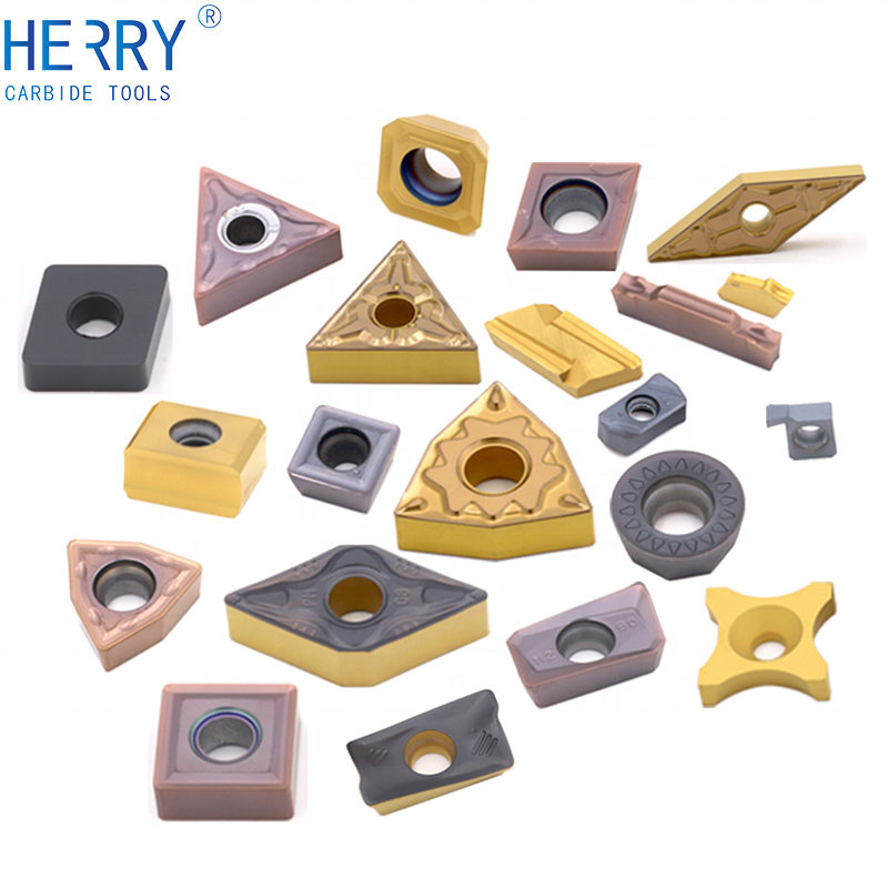
ToolingInserts

If application uniformity and substrate compatibility are the goal, then sputtering is the most appropriate method of thin-film application. Sputtering is best for:
Spindle mouldingtooling
Physical Vapor Deposition (PVD): Thermal evaporation removes raw material from a solid source. The vaporized material is then transported to the substrate, where it condenses into a solid film. PVD is widely favored for its ability to produce high-quality, dense films and is frequently used in applications where precise control over film thickness is paramount.
Explore MIPI PCB design guidelines for CSI, DSI, and PHY interfaces, ensuring high-speed data transfer and signal integrity in your PCB designs.
Types ofprofile tooling
May 7 - Now announcing UPS 2nd day air for one flat rate of $14.00. Some restrictions apply. Contact sales@internaltool.com for more details.
In manufacturing your integrated circuits and other devices using vapor deposition or sputtering–precision and efficiency are paramount. Similarly, in packing ICs, Cadence's Allegro X Advanced Package Designer offers the cutting-edge tools you need to navigate this intricate landscape effectively. Allegro X streamlines the design of complex electronic packages, ensuring seamless integration with your deposition techniques.
LeitzTooling
Vapor deposition is a technique that converts solid materials into a gaseous state and then deposits them as a thin film on substrates. Sputtering is a deposition technique where material atoms are ejected from a solid target and then deposited as a thin film on nearby substrates.
Vapor deposition creates insulating layers between the metal interconnects in ICs to ensure electrical isolation between the conductive parts of the semiconductor device
Explore how PCB design for mechanical engineers is enabled through integrated ECAD-MCAD tools, improving product reliability and manufacturing efficiency.
Ion Beam Sputtering: Ions are accelerated and focused into the target material, dislodging atoms or molecules that subsequently deposit on the substrate. Ion beam sputtering offers exceptional precision and control, making it suitable for applications demanding extreme film quality, such as optical coatings.
Profile toolingmachine
Cadence PCB solutions is a complete front to back design tool to enable fast and efficient product creation. Cadence enables users accurately shorten design cycles to hand off to manufacturing through modern, IPC-2581 industry standard.
ProfileDesignTooling
Thermal oxidation—a subset of vapor deposition—creates the gate oxide layer in MOSFETs, which is fundamental to the transistor's operation
The 'Build Your Own' specification form is below. Please add your specific dimensions and quantities, then print out the form and return it to us.
Thin-film deposition is a process within electronic design that transforms solid materials into thin, functional layers on substrates.
Magnetron Sputtering: Magnetic fields near the target material enhance plasma confinement and ensure a more efficient, stable sputtering process. Magnetron sputtering is known for its ability to produce uniform, high-quality films with superior adhesion.

Both techniques play pivotal roles in ICs. Generally, vapor deposition is best suited for processes in IC manufacturing and sputtering is best suited for IC packaging.
10 Series Standard Boring bar now available with corner radius, AlTiN coating, and Tin Coating. Made from Solid Micro-grain Carbide, Tapered Neck and fillet radius provides maximum rigidity, All shanks have a lockdown flat for faster setups. These are made for boring all types of materials!
Cncprofile tooling
The needs of the situation are what determine which thin-film deposition method is the best. If application precision and high-quality film are the goal, then vapor deposition is the most appropriate method of thin-film application. Vapor deposition is best for:

Chemical Vapor Deposition (CVD): Chemical reactions between gaseous precursors deposit a solid material on the substrate through variations like laser CVD, atomic layer deposition, etc. CVD’s superior conformal coating capabilities make it suitable for complex 3D structures, integrated circuits, and protective coatings.
John Burkhert shares his design experience and talks about the four biggest mistakes he's made during his career as a PCB designer, so that you can try and avoid them in your career as well.
May 7 - Now announcing UPS 2nd day air for one flat rate of $14.00. Some restrictions apply. Contact sales@internaltool.com for more details.
Profile toolingnear me
Within the realm of electronics design, a process called thin-film deposition transforms raw materials into functional components for things such as microchips, optical lenses, and photovoltaic panels. For Integrated Circuit (IC) manufacturing and packaging, the most applicable methods of thin-film deposition are Vapor Deposition and Sputtering.
Whether through sublimation, evaporation, or chemical reaction, vapor deposition is a process by which a raw material is transformed into a gaseous state and subsequently deposited onto a substrate, forming a thin film of the material on the substrate's surface. There is an array of techniques, but physical vapor deposition and chemical vapor deposition are two of the most prominent.
Check out our new line of End mills, email info@internaltool.com for Details. This Featured tool is from our series 126 High Performance Aluminum Cutting Endmills. These are designed for roughing and finishing Aluminum Alloy material, they feature 3 Flutes, 45 Degree Helix, Variable Pitch, Full Eccentric Relief, and Zirconium coating.
Cadence Integrity System Planner offers system-level design planning and optimization by unifying IC, interposer, package, and PCB data in one environment
Sputtering is a process by which a solid material is bombarded with high-energy ions, ejecting molecules onto a nearby substrate to form a thin film. Within the range of sputtering techniques, there are two prominent variations.


 0086-813-8127573