SDS-PAGE: The science behind all those bubbles - sds page diagram
Microfabrication processes widely use CVD to deposit materials in various forms, including: monocrystalline, polycrystalline, amorphous, and epitaxial. These materials include: silicon (dioxide, carbide, nitride, oxynitride), carbon (fiber, nanofibers, nanotubes, diamond and graphene), fluorocarbons, filaments, tungsten, titanium nitride and various high-κ dielectrics.
Hydrogen gas and inert gases such as argon are flowed into the system.[22][26] These gases act as a carrier, enhancing surface reaction and improving reaction rate, thereby increasing deposition of graphene onto the substrate.
Besides these intentional impurities, CVD oxide may contain byproducts of the deposition. TEOS produces a relatively pure oxide, whereas silane introduces hydrogen impurities, and dichlorosilane introduces chlorine.
Chemical vapor deposition (CVD) is a vacuum deposition method used to produce high-quality, and high-performance, solid materials. The process is often used in the semiconductor industry to produce thin films.[1]
CVD is commonly used to deposit conformal films and augment substrate surfaces in ways that more traditional surface modification techniques are not capable of. CVD is extremely useful in the process of atomic layer deposition at depositing extremely thin layers of material. A variety of applications for such films exist. Gallium arsenide is used in some integrated circuits (ICs) and photovoltaic devices. Amorphous polysilicon is used in photovoltaic devices. Certain carbides and nitrides confer wear-resistance.[9] Polymerization by CVD, perhaps the most versatile of all applications, allows for super-thin coatings which possess some very desirable qualities, such as lubricity, hydrophobicity and weather-resistance to name a few.[10] The CVD of metal-organic frameworks, a class of crystalline nanoporous materials, has recently been demonstrated.[11] Recently scaled up as an integrated cleanroom process depositing large-area substrates,[12] the applications for these films are anticipated in gas sensing and low-κ dielectrics. CVD techniques are advantageous for membrane coatings as well, such as those in desalination or water treatment, as these coatings can be sufficiently uniform (conformal) and thin that they do not clog membrane pores.[13]
20231015 — RPM x FPT x Flutes will get a feed rate. Both these formulas won't help much if you don't already know the SFM for different materials. There ...
The direct growth of high-quality, large single-crystalline domains of graphene on a dielectric substrate is of vital importance for applications in electronics and optoelectronics. Combining the advantages of both catalytic CVD and the ultra-flat dielectric substrate, gaseous catalyst-assisted CVD[28] paves the way for synthesizing high-quality graphene for device applications while avoiding the transfer process.
Great for detailed and intricate cuts in thin plastic. The thin, pointed blade allows for precise cutting in small areas.
Silicon nitride deposited by LPCVD contains up to 8% hydrogen. It also experiences strong tensile stress, which may crack films thicker than 200 nm. However, it has higher resistivity and dielectric strength than most insulators commonly available in microfabrication (1016 Ω·cm and 10 MV/cm, respectively).
On the other hand, temperatures used range from 800 to 1050 °C.[22][26] High temperatures translate to an increase of the rate of reaction. Caution has to be exercised as high temperatures do pose higher danger levels in addition to greater energy costs.
CVD is practiced in a variety of formats. These processes generally differ in the means by which chemical reactions are initiated.
The term chemical vapour deposition was coined in 1960 by John M. Blocher, Jr. who intended to differentiate chemical from physical vapour deposition (PVD).
Tungsten CVD, used for forming conductive contacts, vias, and plugs on a semiconductor device,[18] is achieved from tungsten hexafluoride (WF6), which may be deposited in two ways:
Glasses containing both boron and phosphorus (borophosphosilicate glass, BPSG) undergo viscous flow at lower temperatures; around 850 °C is achievable with glasses containing around 5 weight % of both constituents, but stability in air can be difficult to achieve. Phosphorus oxide in high concentrations interacts with ambient moisture to produce phosphoric acid. Crystals of BPO4 can also precipitate from the flowing glass on cooling; these crystals are not readily etched in the standard reactive plasmas used to pattern oxides, and will result in circuit defects in integrated circuit manufacturing.
Choose the right tool for the job based on the type and thickness of the plastic. Consider using a utility knife for thin and flexible plastics, a saw for thicker sheets or pipes, and specialized tools like laser cutters for precision work.
These films have much less tensile stress, but worse electrical properties (resistivity 106 to 1015 Ω·cm, and dielectric strength 1 to 5 MV/cm).[17]
In typical CVD, the wafer (substrate) is exposed to one or more volatile precursors, which react and/or decompose on the substrate surface to produce the desired deposit. Frequently, volatile by-products are also produced, which are removed by gas flow through the reaction chamber.
the decomposition of metal carbonyls is often violently precipitated by moisture or air, where oxygen reacts with the metal precursor to form metal or metal oxide along with carbon dioxide.
Physical conditions such as surrounding pressure, temperature, carrier gas, and chamber material play a big role in production of graphene.
Silicon dioxide (usually called simply "oxide" in the semiconductor industry) may be deposited by several different processes. Common source gases include silane and oxygen, dichlorosilane (SiCl2H2) and nitrous oxide[15] (N2O), or tetraethylorthosilicate (TEOS; Si(OC2H5)4). The reactions are as follows:[16]
Most systems use LPCVD with pressures ranging from 1 to 1500 Pa.[22][27] However, some still use APCVD.[26] Low pressures are used more commonly as they help prevent unwanted reactions and produce more uniform thickness of deposition on the substrate.
Jul 7, 2023 — For NPT threads, tightening with a wrench may allow air leakage after assembly on both large and small diameters, so sealants are used to fill ...
Oxide may also be grown with impurities (alloying or "doping"). This may have two purposes. During further process steps that occur at high temperature, the impurities may diffuse from the oxide into adjacent layers (most notably silicon) and dope them. Oxides containing 5–15% impurities by mass are often used for this purpose. In addition, silicon dioxide alloyed with phosphorus pentoxide ("P-glass") can be used to smooth out uneven surfaces. P-glass softens and reflows at temperatures above 1000 °C. This process requires a phosphorus concentration of at least 6%, but concentrations above 8% can corrode aluminium. Phosphorus is deposited from phosphine gas and oxygen:
Cold wall CVD technique can be used to study the underlying surface science involved in graphene nucleation and growth as it allows unprecedented control of process parameters like gas flow rates, temperature and pressure as demonstrated in a recent study. The study was carried out in a home-built vertical cold wall system utilizing resistive heating by passing direct current through the substrate. It provided conclusive insight into a typical surface-mediated nucleation and growth mechanism involved in two-dimensional materials grown using catalytic CVD under conditions sought out in the semiconductor industry.[31][32]
Quick Tip: One can use any wood working tools to cut acrylic. However, it is very important to take it slow so that the blade doesn't crack the material.
CVD growth allows one to control the properties of the diamond produced. In the area of diamond growth, the word "diamond" is used as a description of any material primarily made up of sp3-bonded carbon, and there are many different types of diamond included in this. By regulating the processing parameters—especially the gases introduced, but also including the pressure the system is operated under, the temperature of the diamond, and the method of generating plasma—many different materials that can be considered diamond can be made. Single-crystal diamond can be made containing various dopants.[35] Polycrystalline diamond consisting of grain sizes from several nanometers to several micrometers can be grown.[33][36] Some polycrystalline diamond grains are surrounded by thin, non-diamond carbon, while others are not. These different factors affect the diamond's hardness, smoothness, conductivity, optical properties and more.
CVD for molybdenum, tantalum, titanium, nickel is widely used.[19] These metals can form useful silicides when deposited onto silicon. Mo, Ta and Ti are deposited by LPCVD, from their pentachlorides. Nickel, molybdenum, and tungsten can be deposited at low temperatures from their carbonyl precursors. In general, for an arbitrary metal M, the chloride deposition reaction is as follows:
For thin sheets of plastic (up to 1/8 inch thick), a simple utility knife can be used. Secure the sheet to a large work surface with a clamp, then use the utility knife to make a straight cut
Aug 10, 2005 — Most reaming feeds and speeds i have seen on manufacturers charts call for 25-30 SFM on mild steel. I've seen that too... but I usually try to ...
Raman spectroscopy, X-ray spectroscopy, transmission electron microscopy (TEM), and scanning electron microscopy (SEM) are used to examine and characterize the graphene samples.[29][30]
Oct 31, 2022 — I will need to source an assortment of cutting bits, and I know that Langmuir is offering cutters, but it always good to have alternatives to compare.
Selecting the right tool for cutting plastic is crucial to achieving accurate and clean results. Consider the type and thickness of the plastic, as well as the desired precision of the cut.
Lower temperature deposition of silicon dioxide and doped glasses from TEOS using ozone rather than oxygen has also been explored (350 to 500 °C). Ozone glasses have excellent conformality but tend to be hygroscopic – that is, they absorb water from the air due to the incorporation of silanol (Si-OH) in the glass. Infrared spectroscopy and mechanical strain as a function of temperature are valuable diagnostic tools for diagnosing such problems.
CVD can be used to produce a synthetic diamond by creating the circumstances necessary for carbon atoms in a gas to settle on a substrate in crystalline form. CVD of diamonds has received much attention in the materials sciences because it allows many new applications that had previously been considered too expensive. CVD diamond growth typically occurs under low pressure (1–27 kPa; 0.145–3.926 psi; 7.5–203 Torr) and involves feeding varying amounts of gases into a chamber, energizing them and providing conditions for diamond growth on the substrate. The gases always include a carbon source, and typically include hydrogen as well, though the amounts used vary greatly depending on the type of diamond being grown. Energy sources include hot filament, microwave power, and arc discharges, among others. The energy source is intended to generate a plasma in which the gases are broken down and more complex chemistries occur. The actual chemical process for diamond growth is still under study and is complicated by the very wide variety of diamond growth processes used.
Silicon nitride is often used as an insulator and chemical barrier in manufacturing ICs. The following two reactions deposit silicon nitride from the gas phase:
The most popular carbon source that is used to produce graphene is methane gas. One of the less popular choices is petroleum asphalt, notable for being inexpensive but more difficult to work with.[22]
Raman spectroscopy is used to characterize and identify the graphene particles; X-ray spectroscopy is used to characterize chemical states; TEM is used to provide fine details regarding the internal composition of graphene; SEM is used to examine the surface and topography.
Cutting plastic may seem like a straightforward task, but the right tools can make a significant difference in achieving precise and clean results. Whether you're a DIY enthusiast, a hobbyist, or involved in industrial applications, selecting the appropriate tool for the job is crucial. In this guide, we'll explore a variety of tools tailored to different plastic-cutting needs.
Other metals, notably aluminium and copper, can be deposited by CVD. As of 2010[update], commercially cost-effective CVD for copper did not exist, although volatile sources exist, such as Cu(hfac)2. Copper is typically deposited by electroplating. Aluminium can be deposited from triisobutylaluminium (TIBAL) and related organoaluminium compounds.
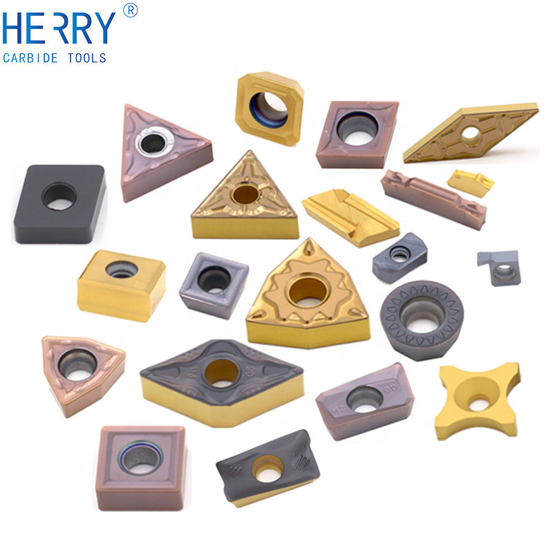
Some code positions relate to the insert that can be used in the toolholder. It's important to remember that the ISO designation system is not a system that ...
In spite of graphene's exciting electronic and thermal properties, it is unsuitable as a transistor for future digital devices, due to the absence of a bandgap between the conduction and valence bands. This makes it impossible to switch between on and off states with respect to electron flow. Scaling things down, graphene nanoribbons of less than 10 nm in width do exhibit electronic bandgaps and are therefore potential candidates for digital devices. Precise control over their dimensions, and hence electronic properties, however, represents a challenging goal, and the ribbons typically possess rough edges that are detrimental to their performance.
The growth of diamond directly on a substrate allows the addition of many of diamond's important qualities to other materials. Since diamond has the highest thermal conductivity of any bulk material, layering diamond onto high heat-producing electronics (such as optics and transistors) allows the diamond to be used as a heat sink.[33][34] Diamond films are being grown on valve rings, cutting tools, and other objects that benefit from diamond's hardness and exceedingly low wear rate. In each case the diamond growth must be carefully done to achieve the necessary adhesion onto the substrate. Diamond's very high scratch resistance and thermal conductivity, combined with a lower coefficient of thermal expansion than Pyrex glass, a coefficient of friction close to that of Teflon (polytetrafluoroethylene) and strong lipophilicity would make it a nearly ideal non-stick coating for cookware if large substrate areas could be coated economically.
Standard quartz tubing and chambers are used in CVD of graphene.[29][30] Quartz is chosen because it has a very high melting point and is chemically inert. In other words, quartz does not interfere with any physical or chemical reactions regardless of the conditions.
Using CVD, films of diamond can be grown over large areas of substrate with control over the properties of the diamond produced. In the past, when high pressure high temperature (HPHT) techniques were used to produce a diamond, the result was typically very small free-standing diamonds of varying sizes. With CVD diamond, growth areas of greater than fifteen centimeters (six inches) in diameter have been achieved, and much larger areas are likely to be successfully coated with diamond in the future. Improving this process is key to enabling several important applications.
Feb 25, 2019 — Hardenability is not a measure of how hard a steel can get. Instead it is a measure of how fast you have to quench to achieve max hardness for a given ...
Fractional Drill Bit, Number Drill Bit, Letter Drill Bit. #0-80, 3/64", -, -. #1-64, -, 53, -. #2-56, -, 50, -. #3-48, -, 47, -. #4-40, 3/32", 43, -. #5-40, - ...
A fine-toothed saw is best for precision cutting of thick plastic. It is particularly useful for making multiple non-linear cuts and yields a smooth finish. This type of saw is recommended for cutting hard plastic.
Feb 4, 2022 — To start, machinists should consult the manufacturers' speeds and feeds charts for the tool and consider decreasing them. Using an end mill with ...
The use of catalyst is viable in changing the physical process of graphene production. Notable examples include iron nanoparticles, nickel foam, and gallium vapor. These catalysts can either be used in situ during graphene buildup,[22][26] or situated at some distance away at the deposition area.[27] Some catalysts require another step to remove them from the sample material.[26]
This reaction is usually performed in LPCVD systems, with either pure silane feedstock, or a solution of silane with 70–80% nitrogen. Temperatures between 600 and 650 °C and pressures between 25 and 150 Pa yield a growth rate between 10 and 20 nm per minute. An alternative process uses a hydrogen-based solution. The hydrogen reduces the growth rate, but the temperature is raised to 850 or even 1050 °C to compensate. Polysilicon may be grown directly with doping, if gases such as phosphine, arsine or diborane are added to the CVD chamber. Diborane increases the growth rate, but arsine and phosphine decrease it.
Commercially, mercury cadmium telluride is of continuing interest for detection of infrared radiation. Consisting of an alloy of CdTe and HgTe, this material can be prepared from the dimethyl derivatives of the respective elements.
If you're looking for precision and quality cuts, Clearly Plastic is an ideal choice. Choosing us ensures that you will have access to a wide range of high-quality plastic materials tailored to your specific requirement. Choosing us will also give you access to our expert guidance and affords you the advantage of our precision cut-to-size services ensuring that you receive your materials tailored to the exact dimensions you require, enhancing convenience and efficiency for your projects.
Provides a rotary blade for smooth and accurate cutting. Excellent for straight lines and curves in materials like vinyl.
Niobium(V) oxide layers can be produced by the thermal decomposition of niobium(V) ethoxide with the loss of diethyl ether[20][21] according to the equation:
Different plastics have varying properties and cutting requirements. Some plastics may melt, chip, or crack more easily than others. Identify the type of plastic you're working with and choose a cutting tool suitable for that specific material.
The choice of source gas depends on the thermal stability of the substrate; for instance, aluminium is sensitive to high temperature. Silane deposits between 300 and 500 °C, dichlorosilane at around 900 °C, and TEOS between 650 and 750 °C, resulting in a layer of low- temperature oxide (LTO). However, silane produces a lower-quality oxide than the other methods (lower dielectric strength, for instance), and it deposits nonconformally. Any of these reactions may be used in LPCVD, but the silane reaction is also done in APCVD. CVD oxide invariably has lower quality than thermal oxide, but thermal oxidation can only be used in the earliest stages of IC manufacturing.
Many variations of CVD can be utilized to synthesize graphene. Although many advancements have been made, the processes listed below are not commercially viable yet.
Speeds and Feeds ... Standard woodruff keyseat cutter sizes with straight or staggered teeth. Product. Number. Teeth. 60000. Straight. 60005. Staggered. 41-Piece ...
Receive two free (adult) ticket vouchers valid for any 2022 HarbourCats regular season home game; Exchange your ticket vouchers at the Victoria HarbourCats' ...
whereas the carbonyl decomposition reaction can happen spontaneously under thermal treatment or acoustic cavitation and is as follows:
Although methane is the most popular carbon source, hydrogen is required during the preparation process to promote carbon deposition on the substrate. If the flow ratio of methane and hydrogen are not appropriate, it will cause undesirable results. During the growth of graphene, the role of methane is to provide a carbon source, the role of hydrogen is to provide H atoms to corrode amorphous C,[23] and improve the quality of graphene. But excessive H atoms can also corrode graphene.[24] As a result, the integrity of the crystal lattice is destroyed, and the quality of graphene is deteriorated.[25] Therefore, by optimizing the flow rate of methane and hydrogen gases in the growth process, the quality of graphene can be improved.


 0086-813-8127573