What is MRR? How to calculate & increase your monthly ... - what is considered a high mrr
PVD is widely used to improve the performance and longevity of cutting tools by providing hard, wear-resistant coatings. Decorative coatings applied via PVD not only enhance the appearance of products but also add a layer of protection. In the optical industry, PVD coatings are used to create anti-reflective surfaces, improving the efficiency and clarity of lenses and mirrors. The ability to apply these coatings precisely and uniformly makes PVD a preferred method for high-performance and high-precision applications.
DNMG insertangle
CVD is integral to the semiconductor industry, providing high-quality dielectric and conductive films essential for device fabrication. Protective coatings deposited by CVD are used to enhance the durability and lifespan of turbine blades in high-temperature and corrosive environments. In the medical field, biocompatible coatings such as titanium nitride improve the performance and longevity of implants and surgical instruments. CVD’s ability to deposit uniform and high-purity films makes it a critical process in advanced technological applications.
Process: Physical Vapor Deposition (PVD) involves the physical transfer of material from a solid or liquid source to a substrate in a vacuum environment. Common techniques include sputtering and evaporation.
WNMGinsert
CVD is well-suited for coating complex geometries, making it ideal for intricate components and internal surfaces. The dense and high-purity coatings produced by CVD enhance material performance in demanding applications. However, the higher temperatures required and the use of hazardous precursor gases necessitate careful handling and sophisticated equipment, increasing the complexity and cost of the process. Despite these challenges, the versatility and quality of CVD coatings make it a preferred choice for many high-performance applications.
DCMTinsert
The lower operating temperatures of PVD make it suitable for coating temperature-sensitive substrates, such as polymers and certain metals. The high vacuum environment minimizes contamination and allows for the deposition of high-purity films. Proper substrate preparation is crucial to achieving strong adhesion and uniform coatings, often involving cleaning, etching, and sometimes heating the substrate.
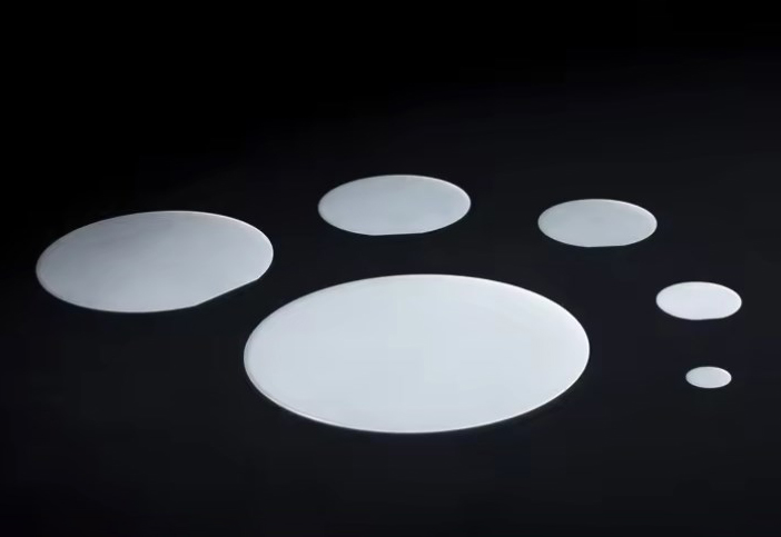
Stanford Advanced Materials (SAM) Corporation is a global supplier of various sputtering targets such as metals, alloys, oxides, ceramic materials. It was first established in 1994 to begin supplying high-quality rare-earth products to assist our customers in the research and development (R&D) fields.
CVD excels in depositing materials that require high purity and precise stoichiometry, such as tungsten for its high melting point and electrical conductivity, and silicon carbide for its thermal and mechanical properties. The ability to deposit diamond films opens up applications in cutting tools and wear-resistant coatings. CVD can also produce composite materials by co-depositing different elements to achieve tailored properties.
PVD is highly versatile, and capable of depositing a wide range of materials including metals, alloys, and ceramics. This versatility makes PVD suitable for applications requiring specific material properties such as hardness, conductivity, and corrosion resistance. For instance, TiN is commonly used for its high hardness and wear resistance, while aluminum oxide is valued for its insulating properties.
VBMTInsert
DNMG InsertHolder
Physical Vapor Deposition (PVD) and Chemical Vapor Deposition (CVD) are prominent coating processes used in various industries to enhance the surface properties of materials. These processes provide protective and functional coatings that improve hardness, wear resistance, and other surface characteristics. This article provides an extensive comparison between PVD and CVD, delving into their mechanisms, applications, advantages, and limitations.
We cannot complete your request due to a technical difficulty. You may return to the previous page or go to the homepage and explore other options. For immediate assistance please call us.
PVD processes are advantageous for producing high-quality coatings with precise control over thickness and composition. The lower operational temperatures and minimal waste production make PVD an environmentally friendly option. However, the need for a high vacuum environment and the line-of-sight limitation can restrict the complexity of the shapes that can be coated. The deposition rates in PVD are generally slower compared to CVD, which can be a drawback in high-volume production scenarios.
CNMGInsert
Physical Vapor Deposition (PVD) and Chemical Vapor Deposition (CVD) offer distinct advantages and are suited for different applications based on their unique properties and process conditions. Understanding these differences allows for informed decisions in selecting the appropriate coating method for specific industrial needs.
VNMGInsert
Process: Chemical Vapor Deposition (CVD) uses chemical reactions to deposit a solid material from a gaseous precursor onto a substrate.
Substrate Preparation: Involves similar cleaning processes but can tolerate more surface imperfections due to chemical reactions.
As technology advances, the development of new deposition techniques and the enhancement of existing ones will likely continue. Research into improving the synthesis and application processes of these materials could lead to even more robust and efficient solutions for industrial challenges. The ongoing exploration of nanotechnology and its integration with deposition techniques holds promise for the next generation of high-performance coatings. Stanford Advanced Materials (SAM) offers sputtering materials and evaporation materials for both PVD and CVD coating processes, ensuring that industries have access to the best resources for their coating needs.
Sputtering involves bombarding a target material with high-energy ions, causing atoms to be ejected and deposited onto the substrate. This method is versatile, allowing for precise control over the film composition and thickness. Evaporation, on the other hand, uses thermal energy to vaporize the material, which then condenses onto the substrate. This process is simpler but may require higher temperatures and is less precise in controlling film properties compared to sputtering.
Details: The higher temperatures required for CVD processes facilitate the necessary chemical reactions but limit the types of substrates that can be coated. Low-pressure CVD (LPCVD) is often used to enhance the quality and uniformity of the coatings, while atmospheric pressure CVD (APCVD) can achieve higher deposition rates. Despite the stringent cleaning requirements, CVD can accommodate some surface imperfections since the chemical reactions can effectively coat irregularities.
Thermal CVD involves heating the substrate and the gaseous precursors, causing the desired reaction to occur at the substrate surface. This method is widely used in the semiconductor industry due to its ability to produce high-purity films. Plasma-Enhanced CVD (PECVD) introduces plasma to lower the reaction temperature, making it suitable for coating heat-sensitive materials. PECVD also allows for better control over film properties and deposition rates.


 0086-813-8127573